Power MOS field effect pipe with poly-silicon field plate and manufacturing method thereof

A technology of polysilicon field plates and field effect transistors, which is applied in transistors, semiconductor/solid-state device manufacturing, electrical components, etc., can solve problems such as edge breakdown of devices, shorten manufacturing time, reduce manufacturing costs, and reduce photolithography times Effect

Inactive Publication Date: 2008-09-24
SUZHOU SILIKRON SEMICON CO LTD
View PDF0 Cites 6 Cited by
  • Summary
  • Abstract
  • Description
  • Claims
  • Application Information

AI Technical Summary

Problems solved by technology

Power MOS field effect transistors need to withstand high reverse voltage during operation. The surface potentials of the parallel unit cell arrays located in the active area in the middle of the device are roughly the same, while the unit cells located at the edge (ie terminal) of the active area and However, the potential on the surface of the substrate varies greatly, which often causes the surface electric field of the outer ring unit cells to be too concentrated, resulting in edge breakdown of the device.

Method used


Image

  • Power MOS field effect pipe with poly-silicon field plate and manufacturing method thereof
  • Power MOS field effect pipe with poly-silicon field plate and manufacturing method thereof
  • Power MOS field effect pipe with poly-silicon field plate and manufacturing method thereof

Examples


Embodiment 1

[0076] Embodiment 1: A power trench MOS field effect transistor

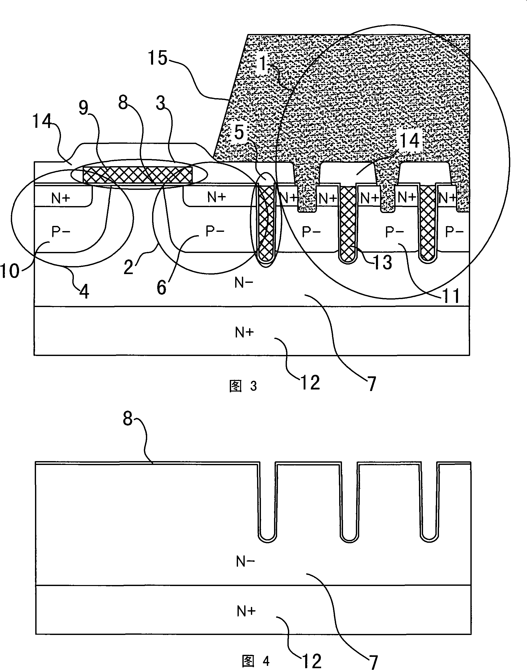
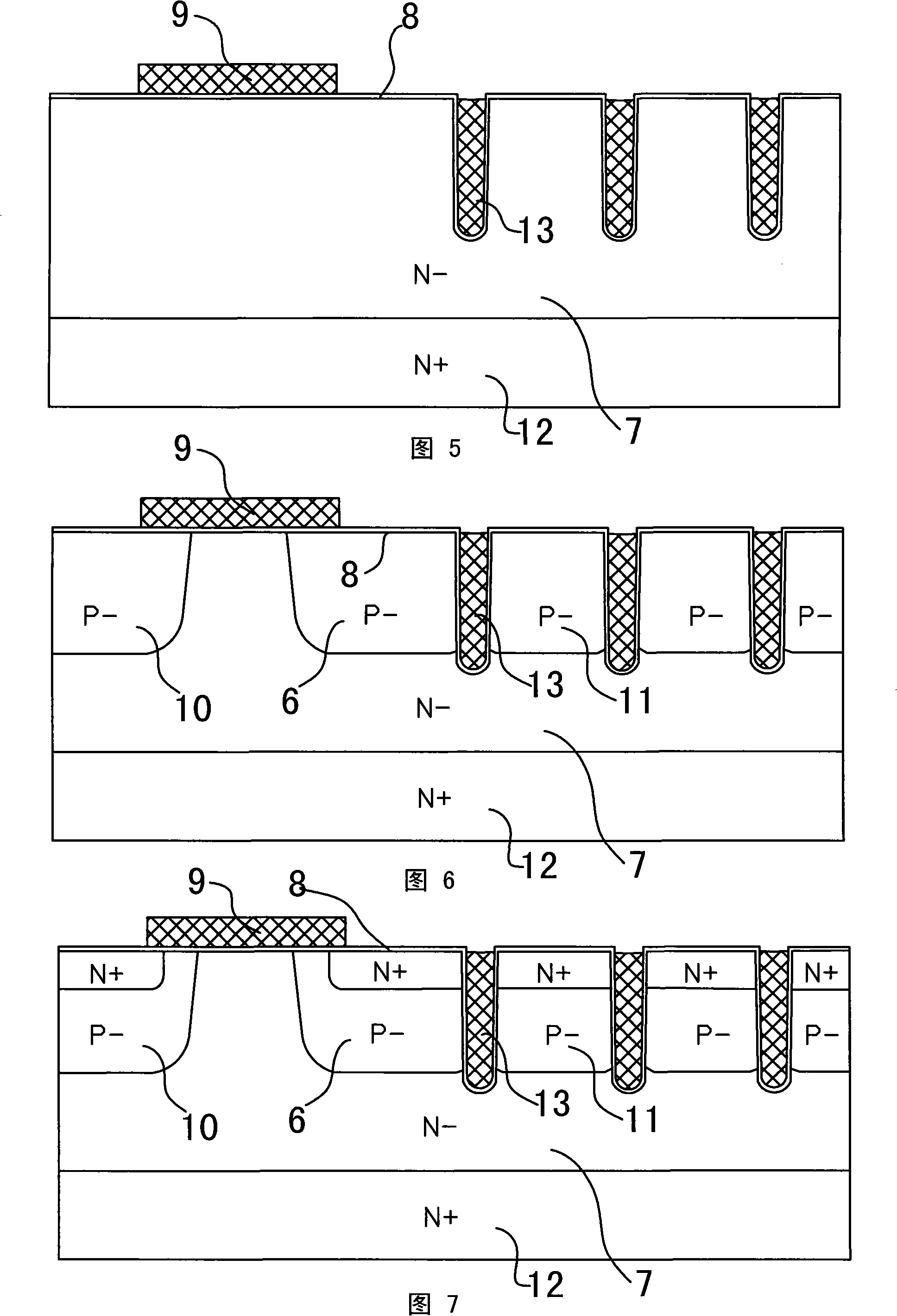
[0077] As shown in Figure 2, on the top plane, the middle of the MOS field effect transistor is a unit cell array 1 connected in parallel, and the periphery of the unit cell array 1 is provided with a terminal protection structure. The MOS field effect transistor is also provided with a gate (in the figure) Not shown), the position of the gate is determined according to the packaging requirements. The terminal protection structure is composed of a field limiting ring 2, a field plate 3 and a stop ring 4.

[0078] As shown in Figure 3, in the cross section, starting from the periphery of the edge unit cell 5 of the active area, the terminal protection structure is arranged in the order of the field limiting ring 2, the field plate 3, and the stop ring 4 from the inside to the outside, and the edge unit cell 5 is directly outside the periphery. Connect the field limit ring 2.

[0079] Field limit ring 2 consists of N ...

Embodiment 2

[0094] Embodiment 2: A power MOS field effect tube

[0095] Such as Picture 10 As shown, the difference between this embodiment and the first embodiment is that the terminal protection structure is composed of two field limiting rings 2, two field plates 3 and one stop ring 4, starting from the periphery of the edge unit cell 5 of the active area, The terminal protection structure is arranged regularly from the inside to the outside according to the field limit ring 2, the field plate 3, the field limit ring 2, the field plate 3, and the final stop ring 4, and the periphery of the edge unit cell 5 is directly connected to the field limit ring 2. The other structure and the content of the manufacturing method are the same as in the first embodiment, and the description is not repeated here.

[0096] From this embodiment, it can be directly derived that the terminal protection structure is composed of three field limiting rings 2, three field plates 3, and one stop ring 4. It can a...


PUM


Abstract

A power MOS field effect transistor with polysilicon field plate and a manufacture method thereof are characterized in that a terminal protection structure of the periphery of an active region of the MOS field effect transistor is improved in the following aspects: 1. a P<-> trap of the periphery of edged unit cells of a unit cell array is directly treated as a field limiting ring; 2. a field limiting ring P<-> area, a cut-off ring P<-> area and a P<-> trap of the unit cell array are treated as the same manufacturing layer which is formed by P-shaped doping simultaneously; 3. field oxygen is omitted, the structure of the field plate is changed in composition and composed by a grid silica layer and polysilicon; 4. the polysilicon in the field plate is treated as a barrier layer injected with P-shaped impurity ions, and the field limiting ring P<-> area, the cut-off ring <-> area and the P<-> trap of the unit cell are formed directly; 5. N-shaped doping is carried out after P-shaped doping, thus causing upper parts of the field limiting ring P<-> area, the cut-off ring P<-> area and the P<-> trap of the unit cell array have an N<+> area. The power MOS field effect transistor with polysilicon field plate and a manufacture method thereof of the invention have the advantages of saving the photoglith plate of the active region, the photoglith plate of the field limiting ring and the photoglith plate with three layers injected in the active region, on the premise of guaranteeing performance of products, reducing times of photoetching, reducing manufacture cost greatly, which are suitable for manufacturing the power MOS field effect transistor with low cost on a large scale.

Description

Technical field [0001] The invention relates to a power MOS field effect tube and a manufacturing method thereof. In particular, it relates to a power MOS field effect tube with a polysilicon field plate and a manufacturing method thereof. This power MOS field effect tube can be an N or P trench type MOS field effect tube, or an N or P plane type MOS field effect tube. The voltage it can withstand is in the medium and low voltage range (20V<voltage<300V). Background technique [0002] Power MOS field effect tubes have been used for many years, and their design and manufacturing methods have been continuously improved. In terms of performance, the development is mainly towards low on-resistance (Rdson), high withstand voltage and high frequency. [0003] The terminal protection structure is a very important part of the MOS field effect tube design. Power MOS field effect transistors need to withstand higher reverse voltages during operation. The surface potentials of the par...

Claims


Application Information

Patent Timeline
Patent Type & Authority Applications(China)
IPC IPC(8): H01L27/088H01L21/8234
Inventor 朱袁正张鲁
Owner SUZHOU SILIKRON SEMICON CO LTD
Why Eureka
Try Eureka