Application of dissoluble tetraalkylammonium axial phthalocyanine compound replacement in making organic film transistor
An organic thin film and tetraalkyl technology, which is applied in the field of optoelectronic materials and information, can solve problems such as harsh conditions, high cost, and complicated processing methods, and achieve the effects of stable performance, adjustable energy level, and easy integrated processing
- Summary
- Abstract
- Description
- Claims
- Application Information
AI Technical Summary
Problems solved by technology
Method used
Image
Examples
Embodiment 1
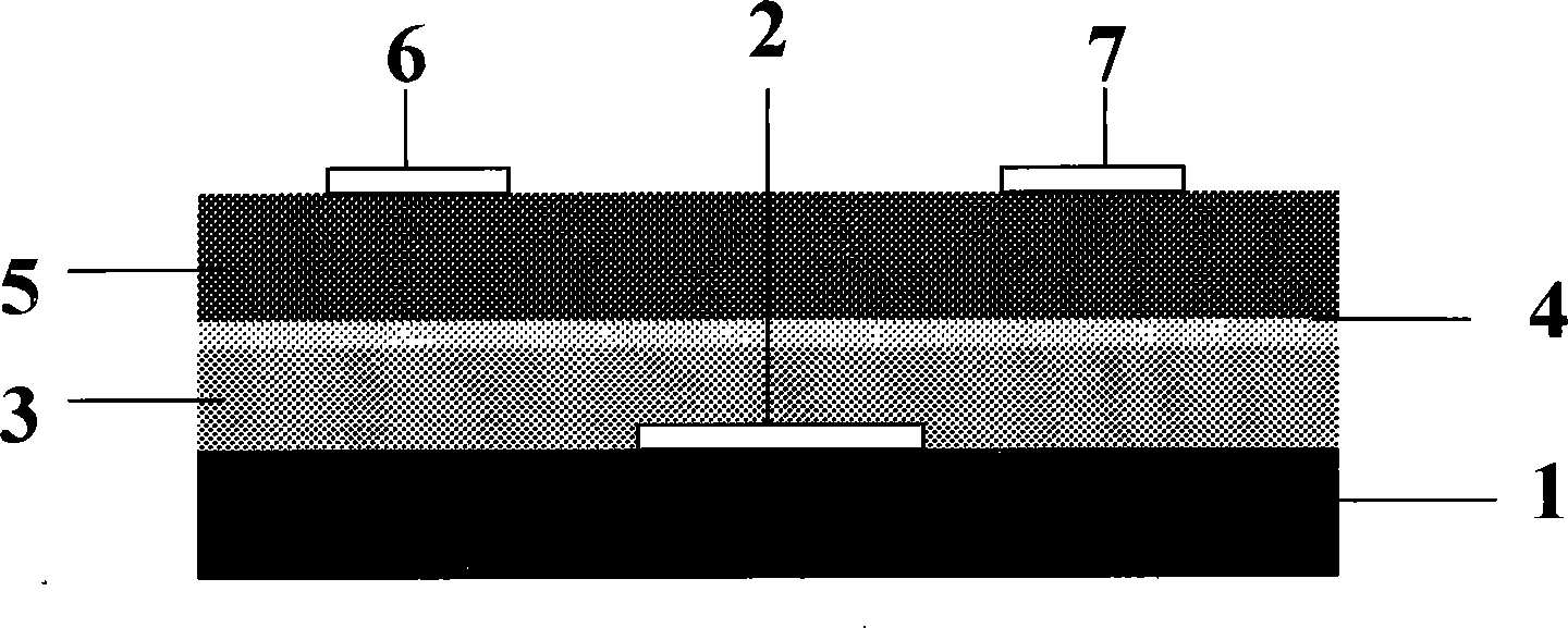
[0029] On the 7059 glass substrate 1, a layer of metal chromium (Cr) film is plated with a radio frequency magnetron sputtering method, with a thickness of 200 nanometers, and it is photoetched into a gate 2; Silicon (SiO 2 ) as the insulating gate layer 3 with a thickness of 100 nanometers, the surface of the insulating gate layer 3 is treated with benzyl trichlorosilane to realize the self-assembled single-layer modification layer 4; The cyanine compounds are:
[0030] 2(3), 9(10), 16(17), 23(24)-tetradodecylphthalocyanine titanium dichloride (TiCl 2 Pc-4C12), 2(3), 9(10), 16(17), 23(24)-tetraoctyltin phthalocyanine dichloride (SnCl 2 Pc-4C8), 2(3), 9(10), 16(17), 23(24)-tetrabutyl phthalocyanine iron chloride (FeClPc-4C4), 2(3), 9(10), 16( 17), 23(24)-tetrapentyl indium phthalocyanine chloride (InClPc), 2(3), 9(10), 16(17), 23(24)-tetraoctyl vanadyl phthalocyanine (VOPc-4C8 ), 2(3), 9(10), 16(17), 23(24)-tetraoctyl phthalocyanine titanium (TiOPc-4C8) or 2(3), 9(10), 16(...
Embodiment 2
[0035] On the 7059 glass substrate 1, a layer of metal chromium (Cr) film is plated by radio frequency magnetron sputtering method, with a thickness of 200 nanometers, and it is photoetched into a grid 2; a layer of trioxide is sputtered on the grid 2 Dialuminum (Al 2 o 3 ) as the insulating gate layer 3, with a thickness of 100 nanometers, on the surface of the insulating gate layer 2, self-assembled single-layer modification layer 4 is carried out with dodecyl phosphoric acid; the soluble tetraalkyl axially substituted phthalocyanine used in the semiconductor layer 5 between the source / drain electrodes The compounds are: 2(3), 9(10), 16(17), 23(24)-tetradodecylphthalocyanine titanium dichloride (TiCl 2 Pc-4C12), 2(3), 9(10), 16(17), 23(24)-tetraoctyltin phthalocyanine dichloride (SnCl 2 Pc-4C8), 2(3), 9(10), 16(17), 23(24)-tetraoctyl phthalocyanine titanium (TiOPc-4C8) or 2(3), 9(10), 16( 17), 23(24)-tetrahexylvanadyl phthalocyanine (SnOPc-4C6), thin film preparation, pos...
Embodiment 3
[0041] On the plastic substrate 1, use the radio frequency magnetron sputtering method to plate one deck metal chromium (Cr) film, thickness 200 nanometers, and photolithography becomes grid 2; Aluminum (Al 2 o 3 ) as the insulating gate layer 3 with a thickness of 100 nanometers; on the surface of the insulating gate layer 3, a butanone solution of 3-0.5wt% PMMA is used to prepare the modified layer 4, and the thickness of the modified layer 4 is 50 nanometers; used for the semiconductor layer 5 between the source / drain electrodes The soluble four-alkyl axially substituted phthalocyanine compounds are 2(3), 9(10), 16(17), 23(24)-tetradodecylphthalocyanine titanium dichloride (TiCl 2 Pc-4C12) or 2(3), 9(10), 16(17), 23(24)-tetraoctylphthalocyanine titanium oxide (TiOPc-4C8), thin film preparation, post-treatment conditions and source and drain electrode processing methods With embodiment 1.
[0042] The source / drain electrodes of the TFT devices, as well as the carrier mobi...
PUM
| Property | Measurement | Unit |
|---|---|---|
| thickness | aaaaa | aaaaa |
| thickness | aaaaa | aaaaa |
| thickness | aaaaa | aaaaa |
Abstract
Description
Claims
Application Information
 - R&D
- Intellectual Property
- Life Sciences
- Materials
- Tech Scout
- Unparalleled Data Quality
- Higher Quality Content
- 60% Fewer Hallucinations
Browse by: Latest US Patents, China's latest patents, Technical Efficacy Thesaurus, Application Domain, Technology Topic, Popular Technical Reports.
© 2025 PatSnap. All rights reserved.Legal|Privacy policy|Modern Slavery Act Transparency Statement|Sitemap|About US| Contact US: help@patsnap.com


