
Method for manufacturing silicon microchannel plate secondary electron emission layer

A secondary electron emission and silicon microchannel plate technology, which is applied in the manufacture of circuits, electrical components, and cold cathodes, can solve problems such as high technical requirements, expensive manufacturing equipment, and long preparation time, and achieve low technical difficulty and smooth process. Simple, short preparation time results

Inactive Publication Date: 2011-06-22
SHENZHEN UNIV
View PDF0 Cites 0 Cited by
  • Summary
  • Abstract
  • Description
  • Claims
  • Application Information

AI Technical Summary

Problems solved by technology

[0009] The technical problem to be solved in the present invention is to provide a method for making a secondary electron emission layer of a silicon microchannel plate, to overcome the existing CVD technology for making a secondary electron emission layer of a silicon microchannel plate, expensive manufacturing equipment, high technical requirements, Drawbacks of long preparation times

Method used


Image

  • Method for manufacturing silicon microchannel plate secondary electron emission layer
  • Method for manufacturing silicon microchannel plate secondary electron emission layer
  • Method for manufacturing silicon microchannel plate secondary electron emission layer

Examples


Embodiment Construction

[0025] Below according to accompanying drawing and embodiment the present invention will be described in further detail:

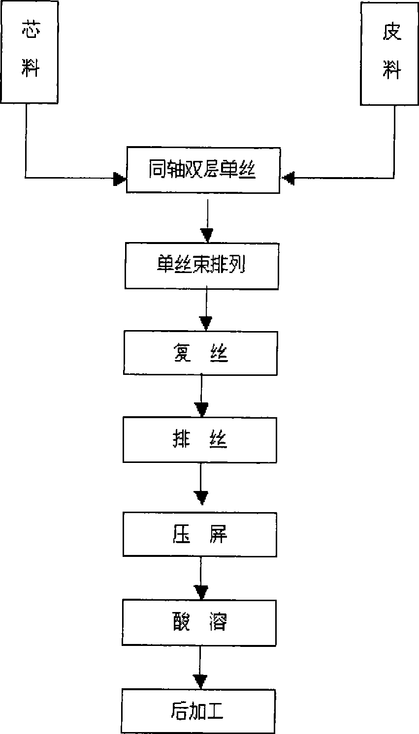
[0026] Considering that the MgO material has a high secondary electron emission coefficient, the secondary electron yield δ value is about 4.5, and the MgO material has good thermal stability, can be directly exposed to the atmosphere, and can be dissolved in a specific solvent No chemical reaction occurs; therefore, the present invention uses MgO as the secondary electron emission material. However, because the melting point of MgO is very high, usually at 3000°C, the conventional vacuum coating method cannot be used; the present invention utilizes the characteristics that MgO is soluble in glacial acetic acid and does not chemically react with glacial acetic acid, according to the ratio of about 1:30 Prepare MgO glacial acetic acid solution. After fully stirring and dissolving, the solution becomes transparent. Place the microchannel plate in the soluti...


PUM

PropertyMeasurementUnit
thicknessaaaaaaaaaa

Abstract

This invention discloses a method for processing secondary electronic emission layers of silicon micro-channel boards including: 1, confecting MgO glacial acetic acid solution in light of a proportion, 2, putting a silicon micro-channel board in the solution to be shaked with supersonic waves for a period of time and enters into the channels fully and is adsorbed on the internal surface, 3, heating the board in a vacuum device to solidify the MgO on the surface.

Description

technical field [0001] The invention relates to the technical field of electric vacuum devices, in particular to a method for manufacturing a silicon microchannel plate (Si-MCP) secondary electron emission layer. Background technique [0002] Microchannel plate (MCP) is a two-dimensional continuous electron multiplication electric vacuum device, which consists of many channels with continuous electron multiplication capabilities arranged in a certain geometric pattern. When a certain electric field is applied to its input and output ends, the extremely weak two-dimensional electron image can be multiplied or enlarged. Since the microchannel plate itself has a certain quantum detection efficiency for most charged particles, some high-energy particles and short-wave light (ultraviolet rays, X-rays, etc.), it can be directly used for detection. Theoretically speaking, micro-channel plates can effectively detect all particles and electromagnetic radiation, so micro-channel plat...

Claims


Application Information

Patent Timeline
Patent Type & Authority Patents(China)
IPC IPC(8): H01J9/02H01J9/00
Inventor 牛丽红
Owner SHENZHEN UNIV
Learn More