Plasma display panel having inert film and manufacturing method

a technology of inert film and display panel, which is applied in the manufacture of electrode systems, electric discharge tubes/lamps, instruments, etc., can solve the problems of surface clouding or decreasing achieve high secondary electron emission coefficient, reduce drive voltage of pdp, and high affinity

Inactive Publication Date: 2014-04-08
MAXELL HLDG LTD
View PDF17 Cites 0 Cited by
  • Summary
  • Abstract
  • Description
  • Claims
  • Application Information

AI Technical Summary

Benefits of technology

[0023]Since a metal such as a rare-earth metal has a high affinity for oxygen, it traps carbon dioxide and moisture vapor in the atmosphere to prevent the carbon dioxide and the moisture vapor from penetrating the underlayer surface of materials having a high secondary electron emission coefficient. As a result, a high γ material surface is kept clean after the inert film has been removed. Since the secondary electron emission from a clean high γ material occurs in a low voltage, a reduction in drive voltage of the PDP is made possible.
[0024]In addition, since the present invention allows formation of an inert film having outstanding barrier properties, SrO, CaO, BaO or a mixture including them, which cannot be conventionally easily used for a protective film, can be used for the protective film. Since these films of them have a higher secondary electron emission coefficient than that of MgO, a plasma display panel in which the discharge voltage is low can be achieved.

Problems solved by technology

However, MgO is deliquescent and therefore exposure of it to the air transforms the surface of the protective film, thus making the surface become clouded or decreasing the secondary electron emission coefficient.

Method used


Image

  • Plasma display panel having inert film and manufacturing method
  • Plasma display panel having inert film and manufacturing method
  • Plasma display panel having inert film and manufacturing method

Examples


example 1

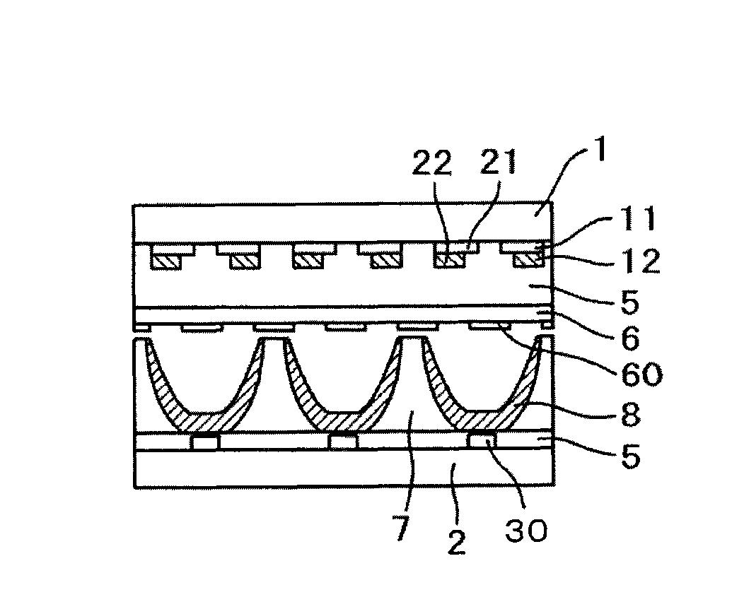
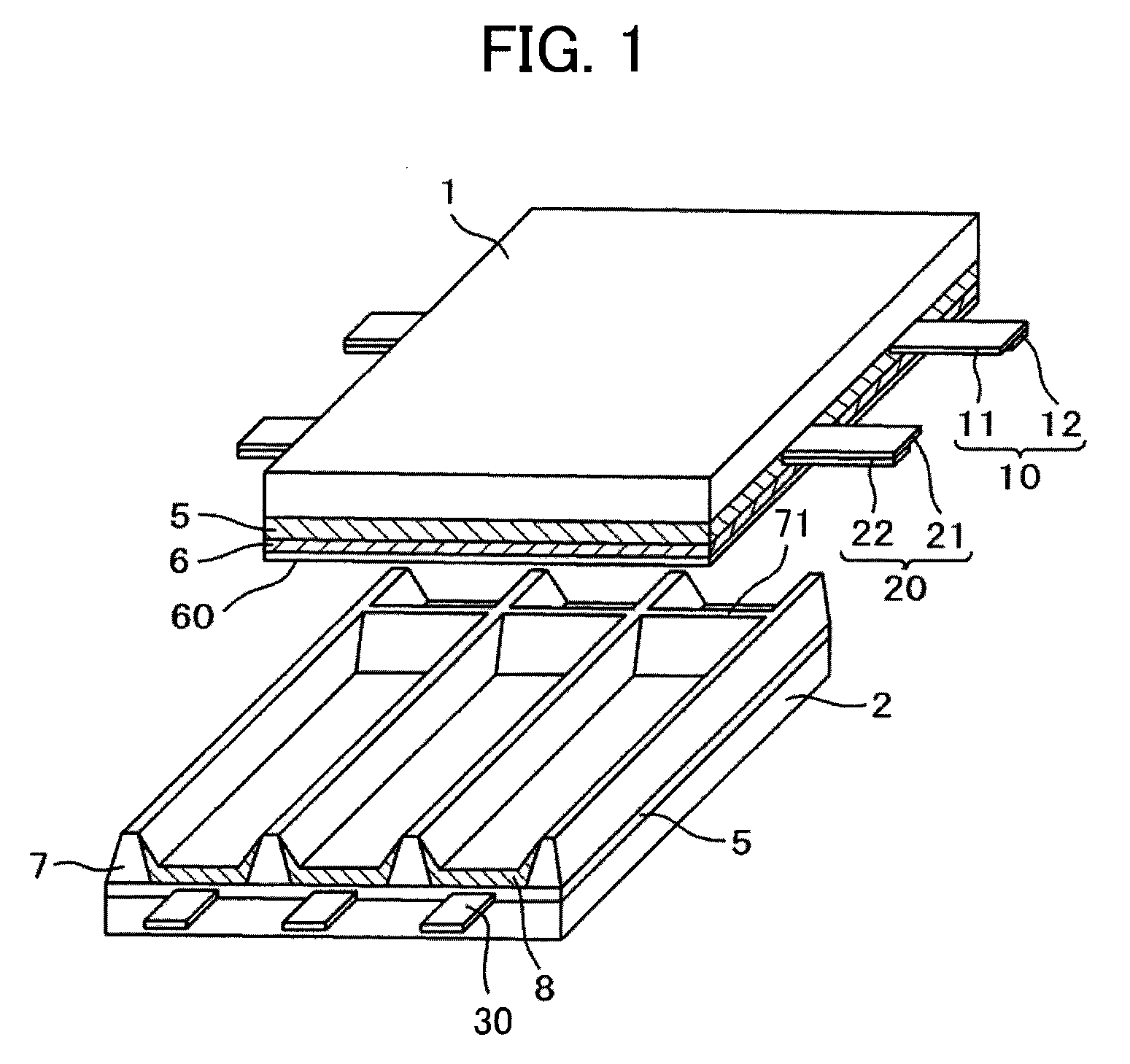
[0026]FIG. 1 is an exploded perspective view of the display area of a plasma display panel. The plasma display panel includes two glass substrates, a front substrate 1 and a back substrate 2. On the front substrate 1 each of scan electrodes 20 (hereinafter also called “Y electrode(s) 20”) and each of discharge sustain electrodes 10 (hereinafter also called “X electrode(s) 10”), between which a discharge is generated for image formation, are arranged parallel.

[0027]The scan electrode 20 in turn includes a scan discharge electrode which is made of ITO (Indium Tin Oxide) and operates actually as a discharge electrode, and a scan bus electrode which is provided for supplying voltage from a terminal. In the following, the scan bus electrode is also called a Y bus electrode 22, and the scan discharge electrode is also called a Y discharge electrode 21. Note that if the “Y electrode 20” is simply described, this means the Y electrode 20 including the Y bus electrode 22 and the Y discharge ...

example 2

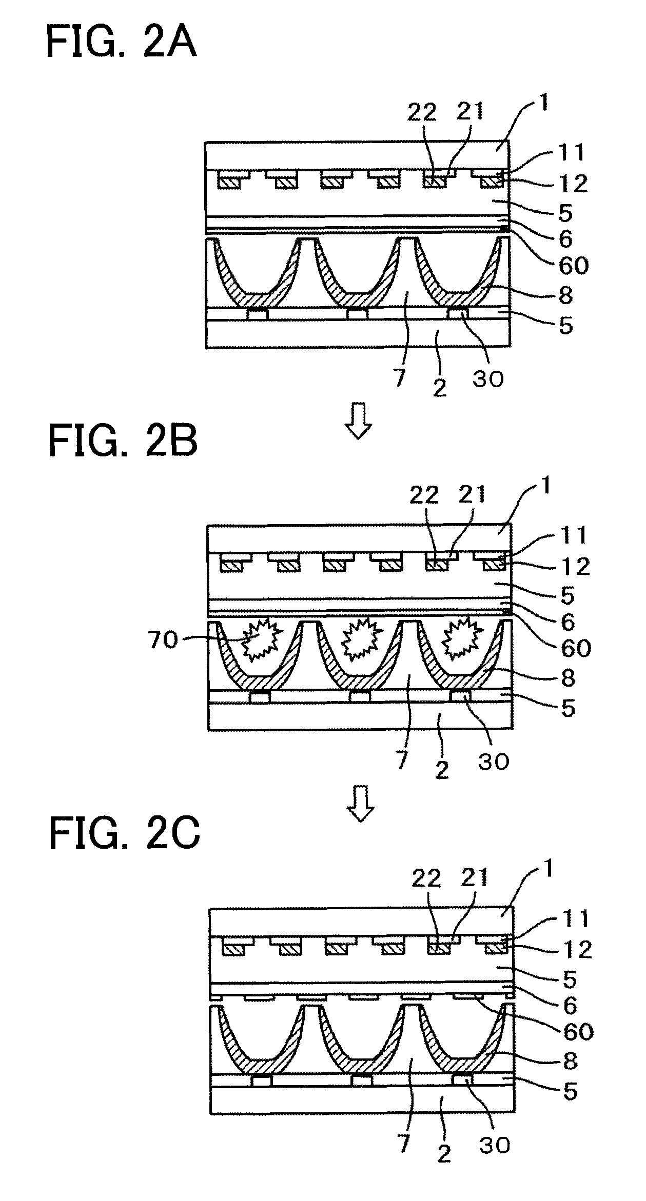
[0055]A plasma display panel made in the example is similar in structure to the plasma display panel made in Example 1. This example differs in a method of producing an inert film 60 from Example 1. FIG. 4 shows the method of producing an inert film 60 according to this example. In Example 1, the mixture of SiO2 and Tb is placed in the substrate hearth 200 and then is heated by an electron beam to form a film. In contrast to this, in this example, a SiO2 film and Tb are placed in different hearths and are respectively heated by electron beams for vapor deposition.

[0056]SiO2 and Tb differ in vapor deposition rate. In this example, however, since SiO2 and Tb can be independently controlled for vapor deposition, a mixing ratio of two types of vapor-deposition components can be accurately controlled. The front substrate 1 with an evaporated inert film 60 is moved in the direction shown by the arrow in FIG. 4 to be exposed to the atmosphere, which is the same as FIG. 3 in Example 1.

[0057...

example 3

[0058]A plasma display panel made in the example is similar in structure to the plasma display panel made in Example 1. This example differs in a method of producing an inert film 60 from Examples 1 and 2. In Examples 1 and 2, vacuum vapor deposition is used to form the inert film 60. In this example, however, sputtering is used to form the inert film 60.

[0059]FIG. 5 is an example showing a method of forming the inert film 60 according to this example. In FIG. 5, as a sputtering target 300, one with Tb implanted in a SiO2 target is used. In this regard, in a sputtering technique as shown in FIG. 5, sputtering can also be performed when Tb pieces are placed on the SiO2 target. In FIG. 5, SiO2 and Tb sputtered from the sputtering target 300 adhere to the front substrate 1 which is set to the substrate setting jig 100 provided above them.

[0060]In FIG. 5, the front substrate 1 is placed in a downward direction. However, a feature of the sputtering technique is that a substrate can be ve...


PUM

PropertyMeasurementUnit
thicknessaaaaaaaaaa
voltageaaaaaaaaaa
softening pointaaaaaaaaaa

Abstract

A protective film (6) having a high secondary-emission coefficient is formed on a dielectric layer (5) so as to lower the discharge voltage of a plasma display panel. When the protective film (6) is exposed to the air, it will transform or become cloudy, or the secondary-emission coefficient will lower. To prevent this problem, an inert film (60) is formed on the surface of the protective film (6). As the inert film (60), a film of a metal oxide such as SiO2 and a film of a metal such as Tb are simultaneously formed. Thus, an inert film (60) excellent in barrier property against oxygen and water in the air and enabling easy sputtering from near the discharge electrode at the aging step can be obtained. With this, a plasma display panel exhibiting a low discharge voltage can be realized.

Description

TECHNICAL FIELD[0001]This invention relates to a display device, and relates to a structure of a plasma display panel capable of operating at a reduced discharge voltage and a method for manufacturing the plasma display panel.BACKGROUND ART[0002]The demand for PDP display devices using a plasma display panel (PDP) grows as a flat display capable of large-screen displays. The PDP display device includes a plasma display panel, a front panel placed on the front of the plasma display panel, a drive circuit placed on the back of the plasma display panel, a frame containing them, and the like.[0003]On the front substrate scan electrodes extend from, for example, the left-hand end of the front substrate to the display area, while discharge-sustain electrodes extend from, for example, the right-hand end of the front substrate to the display area. On the back substrate, address electrodes each extend in a direction at right angles to the scan electrode and the discharge-sustain electrode. S...

Claims


Application Information

Patent Timeline
Patent Type & Authority Patents(United States)
IPC IPC(8): H01J11/12H01J11/38H01J17/49H01J11/40
CPCH01J9/02H01J11/12H01J11/38H01J11/40
Inventor HASEGAWA, MINORUFUKUTA, SHINYABETSUI, KEIICHIHASHIMOTO, YASUNOBU
Owner MAXELL HLDG LTD
Why Eureka
Try Eureka