
Plasma display panel

A display panel and plasma technology, which is applied to alternating current plasma display panels, discharge tubes, electrical components, etc., can solve the problems of long aging time, inability to be practical, and reduced secondary electron emission coefficient, and achieves long life of driving voltage, The effect of low drive voltage

Inactive Publication Date: 2011-10-12
PANASONIC CORP
View PDF2 Cites 0 Cited by
  • Summary
  • Abstract
  • Description
  • Claims
  • Application Information

AI Technical Summary

Problems solved by technology

If such a compound is formed, the secondary electron emission coefficient of the protective layer decreases, and the discharge start voltage and sustain voltage cannot be lowered as expected, or the aging time required for the voltage drop becomes very long, and there is a problem that it cannot be practically used.

Method used


Image

  • Plasma display panel
  • Plasma display panel
  • Plasma display panel

Examples


Embodiment 1

[0085] In this example, the In 2 o 3 React with CaO, SrO, BaO, and rare earth metal oxides to synthesize electron-emitting materials (crystalline compounds) and conduct experiments to confirm the effect of improving chemical stability.

[0086] (Synthesis of crystalline compounds)

[0087] As a starting material, as a reagent special grade or higher CaCO 3 , SrCO 3 、BaCO 3 , a representative of rare earth metal oxides, using La 2 o 3 , Y 2 o 3 , and In 2 o 3 . These raw materials were weighed so that the molar ratio of each metal ion became the value shown in Table 1, wet mixed using a ball mill, and dried to obtain mixed powder. Among them, since only No.6 is In 2 o 3 , so mixing treatment etc. are not particularly performed, nor is subsequent sintering performed.

[0088]Put their mixed powder into an alumina crucible, and sinter in air at 1000-1300°C for 2 hours in an electric furnace. The average particle diameter of the obtained powder was measured, and for...


PUM


Abstract

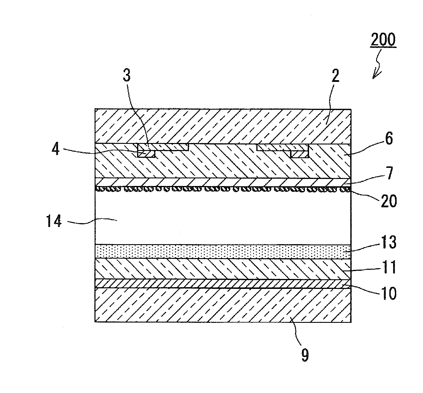
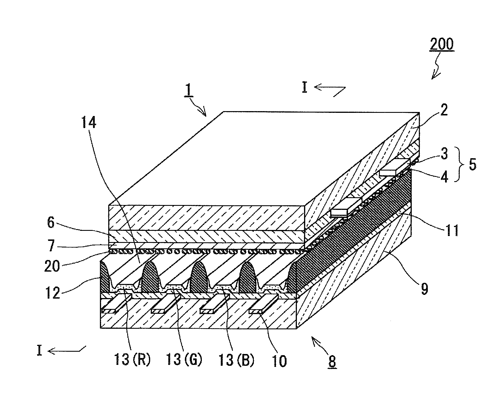
A material suitable for improving the coefficient of secondary-electron emission of PDPs (Plasma Display Panel) is provided to thereby enable a PDP to operate at a higher efficiency. Provided is a PDP (200) which includes a protective layer (7) constituted of MgO and an electron-emitting layer (20) formed on the protective layer (7), the electron-emitting layer (20) comprising electron-emitting particles constituted of a crystalline compound that have been spread on the protective layer (7). The electron-emitting particles are a crystalline compound comprising as major components: one or more elements selected from calcium, strontium, barium, and rare-earth metals; indium; and oxygen.

Description

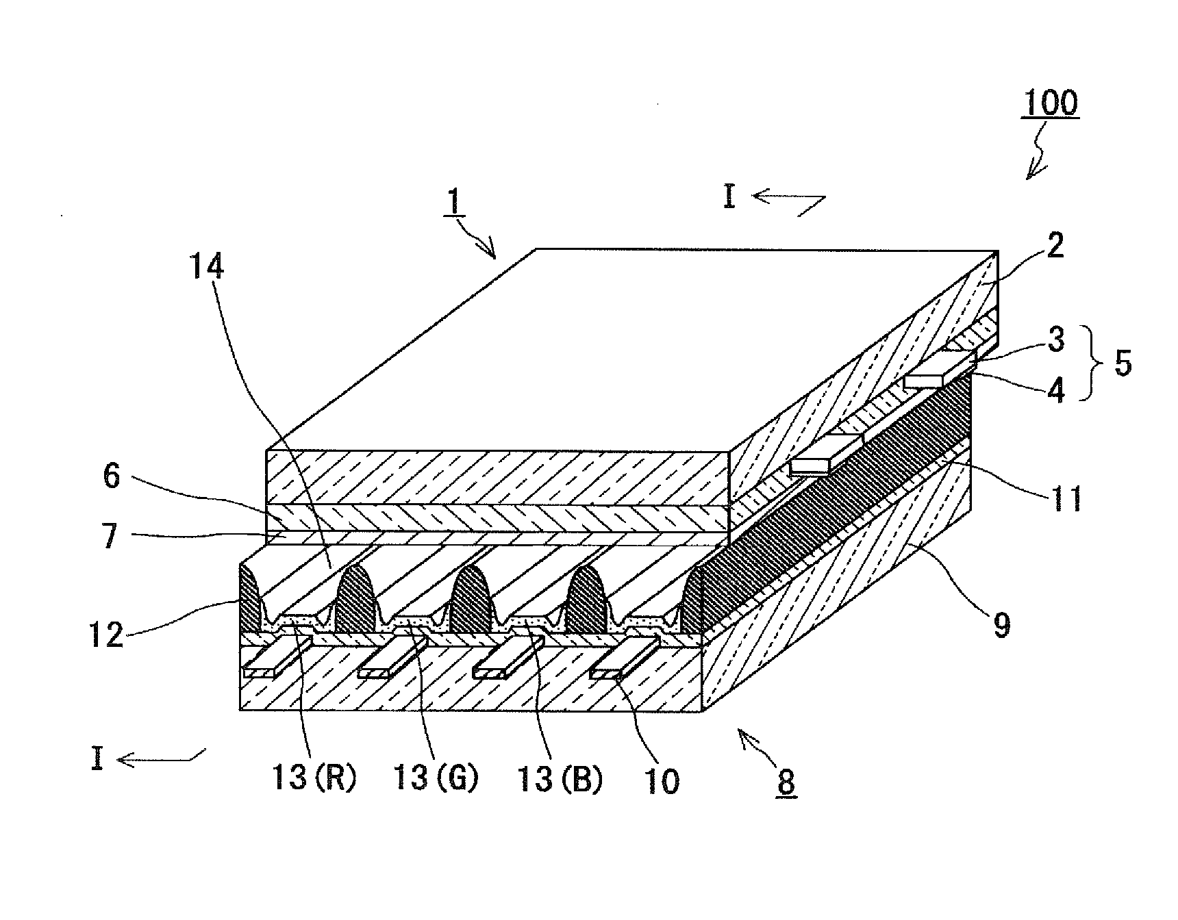
technical field [0001] The present invention relates to a plasma display panel (PDP). Background technique [0002] Plasma display panels (hereinafter abbreviated as PDPs) have the characteristics of easy enlargement, high-speed display, and low cost among thin display panels, so they have been put into practical use and rapidly popularized. [0003] The structure of a common PDP that has been put into practical use is to arrange two glass substrates facing each other as a front substrate and a rear substrate, respectively provide a pair of electrodes arranged regularly, and provide a dielectric such as low-melting glass to cover these electrodes. layer. Furthermore, a phosphor layer is provided on the dielectric layer of the rear substrate, and a protective layer made of MgO is provided on the dielectric layer of the front substrate to protect the dielectric layer from ion impact and improve secondary electron emission. Furthermore, a gas mainly composed of an inert gas s...

Claims


Application Information

Patent Timeline
Patent Type & Authority Applications(China)
IPC IPC(8): H01J11/02H01J11/12H01J11/40
CPCH01J11/12H01J11/40H01J17/49
Inventor 井上修浅野洋奥井弥生奥山浩二郎白石诚吾
Owner PANASONIC CORP
Learn More