MgO dual-potential magnetic tunnel structure with quanta effect and its purpose
A magnetic tunnel junction and quantum effect technology, which is applied in the fields of magnetic field controlled resistors, spin exchange coupled multi-layer films, static memories, etc., to achieve the effect of performance improvement
- Summary
- Abstract
- Description
- Claims
- Application Information
AI Technical Summary
Problems solved by technology
Method used
Image
Examples
Embodiment 1
[0027] Example 1. Preparation of MgO Double Barrier Magnetic Tunnel Junction with Quantum Effect by Mg Oxidation Method
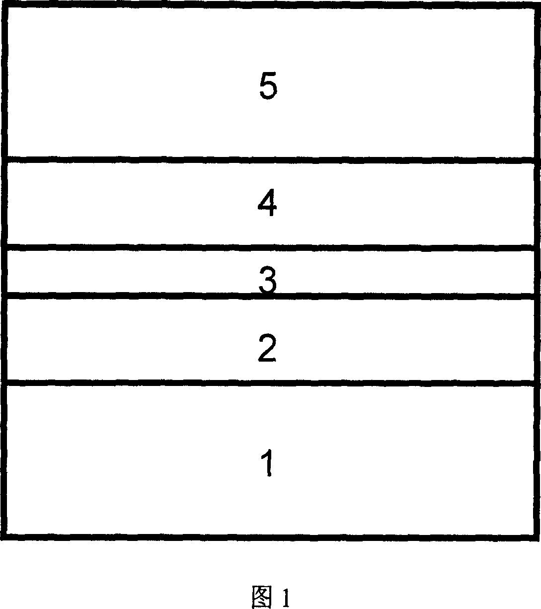
[0028] Using high-vacuum magnetron sputtering equipment on Si / SiO cleaned by conventional methods 2 On the substrate, a lower buffer conductive layer Ta with a thickness of 10nm; an antiferromagnetic pinning layer Ir-Mn with a thickness of 15nm; and a five-layer core film layer (M1 / I1 / M / I2 / M2)——Fe( 10nm) / MgO(2nm) / Fe(1nm) / MgO(2nm) / Fe(10nm); continue to deposit a 12nm antiferromagnetic Ir-Mn pinning layer and a 10nm Au top protective layer on top of the core film layer. The MgO insulating layer in the core film layer is formed by depositing 2nm metal Mg and oxidizing it by plasma for 30 seconds. The growth conditions of the above-mentioned magnetic multilayer film: prepared vacuum: 5×10 -7 Pa; high-purity argon gas pressure for sputtering: 0.07Pa; sputtering power: 120W; sample holder rotation rate: 20rmp; growth temperature: room temperature; growth rate: ...
Embodiment 2
[0030] Example 2, MgO (001) target direct sputtering method to prepare MgO double barrier magnetic tunnel junction with quantum effect
[0031] Utilize the high-vacuum magnetron sputtering equipment to sequentially deposit the lower buffer conductive layer Ru with a thickness of 10nm on the single crystal MgO(001) material substrate cleaned by conventional methods; the antiferromagnetic pinning layer Pt-Mn of 12nm; and five Core layer of layer structure (M1 / I1 / M / I2 / M2)-Co(15nm) / MgO(4nm) / Co(2nm) / MgO(4nm) / Co(15nm); continue above the core layer A 12 nm antiferromagnetic pinning layer Pt-Mn and a top 5 nm Pt protective layer were deposited. The MgO insulating layer in the core film layer is formed by direct sputtering of (001) single crystal MgO target. The growth conditions of the above-mentioned magnetic multilayer film: prepared vacuum: 5×10 -7 Pa; high-purity argon gas pressure for sputtering: 0.07Pa; sputtering power: 120W; sample holder rotation rate: 20rmp; growth temper...
Embodiment 3
[0033] Example 3, MgO and metal co-sputtering method to prepare doped MgO double barrier magnetic tunnel junction with quantum effect
[0034] Utilize the high-vacuum magnetron sputtering equipment to successively deposit on the GaAs material substrate that is cleaned by conventional methods a lower buffer conductive layer Ta with a thickness of 15nm; an antiferromagnetic pinning layer PtCr with a thickness of 12nm; and a five-layer core film layer (M1 / I1 / M / I2 / M2)-Co-Fe-B(20nm) / MgO(3nm) / Co-Fe(2nm) / MgO(3nm) / Co-Fe-B(20nm); above the core film layer Continue to deposit 10 nm of antiferromagnetic pinning layer PtCr and top 5 nm of Cr protection layer. The MgO insulating layer in the core film layer is doped with Al, which is formed by co-sputtering of (001) single crystal MgO target and metal Al target. The purpose is to reduce the resistance of the double barrier tunnel junction, and the Al doping content is 3% ( adjustable). The growth conditions of the above-mentioned magnet...
PUM
| Property | Measurement | Unit |
|---|---|---|
| thickness | aaaaa | aaaaa |
| thickness | aaaaa | aaaaa |
| thickness | aaaaa | aaaaa |
Abstract
Description
Claims
Application Information
 - Generate Ideas
- Intellectual Property
- Life Sciences
- Materials
- Tech Scout
- Unparalleled Data Quality
- Higher Quality Content
- 60% Fewer Hallucinations
Browse by: Latest US Patents, China's latest patents, Technical Efficacy Thesaurus, Application Domain, Technology Topic, Popular Technical Reports.
© 2025 PatSnap. All rights reserved.Legal|Privacy policy|Modern Slavery Act Transparency Statement|Sitemap|About US| Contact US: help@patsnap.com


