Micro flow control chip device for liquid surface tension detection
A liquid surface tension, microfluidic chip technology, applied in the direction of surface tension analysis, etc., can solve a large number of samples, microfluidic chip devices without liquid surface tension, can not meet the high throughput and other problems, to achieve easy waterproof treatment, Avoid the effect of precise adjustment and convenient measurement
- Summary
- Abstract
- Description
- Claims
- Application Information
AI Technical Summary
Problems solved by technology
Method used
Image
Examples
Embodiment 1
[0058] 1) Mask design of substrate 1:
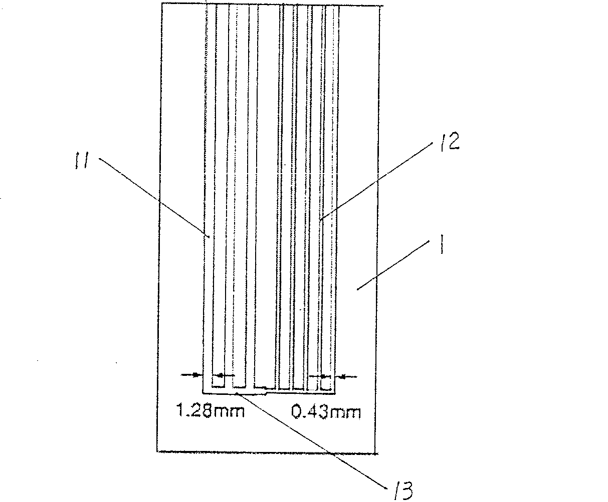
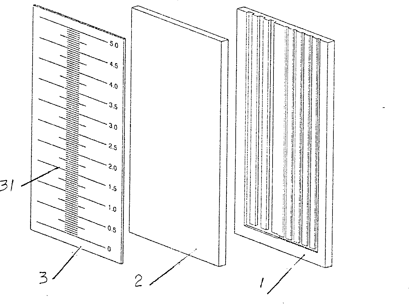
[0059] The structure and size design of the groove on the mask film are as attached figure 1 shown. 3 wide vertical first grooves 11 and 5 narrow vertical second grooves 12 are arranged in parallel, and the widths are respectively 0.6mm and 0.15mm. The groove 11 communicates with the vertical second groove 12 and the vertical third groove 13 at the end, and the width of the third horizontal groove 13 is 0.15mm. The number of the first vertical groove 11 and the second vertical groove 12 can be appropriately increased or decreased to control the amount of sample used.
[0060] 2) The making of substrate 1:
[0061] Place the mask film on a 63mm×31.5mm×1.5mm leveling chrome plate and press it tightly, expose it to an ultraviolet lamp with a wavelength of 365nm for 200 seconds, and then develop it in 0.5% sodium hydroxide developer for 40 seconds. After washing with deionized water, heat at 100°C for half an hour. Use chromium etching ...
Embodiment 2
[0065] 1) Mask design of substrate 1:
[0066] The structure and size design of the groove on the mask film are as attached figure 1 shown. 3 wide vertical first grooves 11 and 5 narrow vertical second grooves 12 are arranged in parallel, and the widths are respectively 0.6mm and 0.15mm. The groove 11 communicates with the vertical second groove 12 and the vertical third groove 13 at the end, and the width of the third horizontal groove 13 is 0.15 mm. The number of the first vertical groove 11 and the second vertical groove 12 can be appropriately increased or decreased to control the amount of sample used.
[0067] 2) The making of substrate 1:
[0068] Place the mask film on a 63mm×31.5mm×1.5mm leveling chrome plate and press it tightly, expose it to an ultraviolet lamp with a wavelength of 365nm for 200 seconds, and then develop it in 0.5% sodium hydroxide developer for 40 seconds. After washing with deionized water, heat at 100°C for half an hour. Use chromium etching...
Embodiment 3
[0072] 1) Mask design of substrate 1:
[0073] The structure and size design of the groove on the mask film are as attached figure 1 shown. 3 wide vertical first grooves 11 and 5 narrow vertical second grooves 12 are arranged in parallel, and the widths are respectively 0.6mm and 0.15mm. The groove 11 communicates with the vertical second groove 12 and the vertical third groove 13 at the end, and the width of the third horizontal groove 13 is 0.15 mm. The number of the first vertical groove 11 and the second vertical groove 12 can be appropriately increased or decreased to control the amount of sample used.
[0074] 2) The making of substrate 1:
[0075] Place the mask film on a 63mm×31.5mm×1.5mm leveling chrome plate and press it tightly, expose it to an ultraviolet lamp with a wavelength of 365nm for 200 seconds, and then develop it in 0.5% sodium hydroxide developer for 40 seconds. After washing with deionized water, heat at 100°C for half an hour. Use chromium etching...
PUM
| Property | Measurement | Unit |
|---|---|---|
| area | aaaaa | aaaaa |
| area | aaaaa | aaaaa |
| area | aaaaa | aaaaa |
Abstract
Description
Claims
Application Information
 - R&D Engineer
- R&D Manager
- IP Professional
- Industry Leading Data Capabilities
- Powerful AI technology
- Patent DNA Extraction
Browse by: Latest US Patents, China's latest patents, Technical Efficacy Thesaurus, Application Domain, Technology Topic, Popular Technical Reports.
© 2024 PatSnap. All rights reserved.Legal|Privacy policy|Modern Slavery Act Transparency Statement|Sitemap|About US| Contact US: help@patsnap.com


