
Direct bonding method for indium phosphide and gallium arsenide materials

A direct bonding, direct technology, used in lasers, electrical components, circuits, etc., can solve problems such as large limitations and poor conductivity

Inactive Publication Date: 2007-12-19
SHANGHAI INST OF MICROSYSTEM & INFORMATION TECH CHINESE ACAD OF SCI
View PDF0 Cites 11 Cited by
  • Summary
  • Abstract
  • Description
  • Claims
  • Application Information

AI Technical Summary

Problems solved by technology

[0007] Literature [3] [H.C.Lin, K.L.Chang, G.W.Pickrell, K.C.Hsieh, and K.Y.Cheng, Low temperature wafer bonding by spin on glass, J.Vac.Sci.Technol.B Vol.20 No.2., 752(2002 )] introduces the use of Spin on glass (SOG) media to bond InP and GaAs materials. SOG is a solution of silanol and methyl polymers in alcohol. Although the bonding temperature is low, due to the bonding media It has the disadvantages of certain thickness, poor conductivity, light absorption, etc., so it has great limitations

Method used


Image

  • Direct bonding method for indium phosphide and gallium arsenide materials

Examples


Embodiment 1

[0027] The process steps for the direct bonding of InP and GaAs are:

[0028] 1. Cleavage the InP and GaAs substrates into a square with a side length of 2.5cm;

[0029] 2. Cleaning the substrate: use isopropanol, acetone and absolute ethanol to ultrasonically clean the sample piece 3 times each for 5 minutes, and then rinse with deionized water for more than 3 minutes;

[0030] 3. To remove surface oxides: InP is at rest H 2 SO 4 +H 2 O 2 +H 2 O (volume ratio is 3:1:1) in the corrosion for 10 seconds, GaAs in the static H 2 SO 4 +H 2 Etch in O (volume ratio 1:20) for 40 seconds. Before etching, both InP and GaAs need to be blown dry with high-purity nitrogen. After the etching is completed, rinse with deionized water for more than 5 minutes; Blow dry with high purity nitrogen and immerse directly into HF+H 2 Soak in O (volume ratio 1:10) for 30 seconds, and then rinse with deionized water three times; the above corrosion processes are all completed at room temperature (20~25℃);

...

Embodiment 2

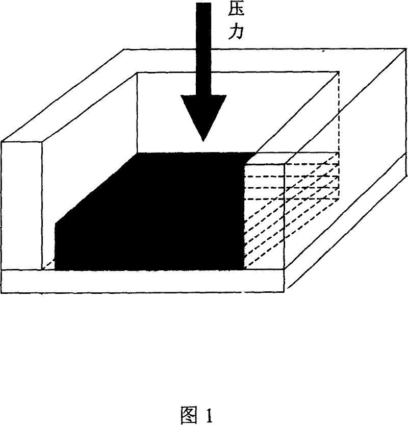
[0037] In this embodiment, InP and GaAs are cleaved into a rectangular shape, with side lengths of 1.5 cm and 2.5 cm, respectively, and the edge-to-side alignment overlap angle is 1°. The bonding temperature is 680℃, and the pressure applied after keeping for 30 minutes is 2Kg / cm. 2 , The cooling rate in the temperature range of 680-450℃ is 3.5℃ / min, the cooling rate in the range of 450-300℃ is 2℃ / min, and the rest is the same as in Example 1.


PUM


Abstract

The invention relates to direct bonding method of InP and GaAs including thee technical processes of surface cleaning, laminating and high-temp annealing. The characteristic is that surface of InP and GaAs is processed two times by deoxidizing before bonding, then it is direct soaked in reducibility nitrogen solution without drying by high-purity nitrogen, after being soaked, it is direct put into anti-oxide alcohol solution. Laminate is processed in the alcohol solution, burnishing surface of InP is downward to be put on burnishing surface of GaAs straight, InP and GaAs are coincided together that side and side are aligned, bonding temp. is from 500 to 700 deg.C, annealed after being bonded, keeping time is from 30 to 40 minutes, both bonding and annealing are proceeded by nitrogen protection. Optical and electrical performance of whole material structure can not be reduced since the bonded IP and GaAs interface.

Description

Technical field [0001] The invention provides a direct bonding method of III-V compound semiconductor indium phosphide (InP) and gallium arsenide (GaAs) materials, and belongs to the technical field of semiconductor optoelectronics and microelectronic device technology. Background technique [0002] With the development of semiconductor material epitaxy technologies such as molecular beam epitaxy (MBE), metal organic chemical vapor deposition (MOCVD) and other technologies, the growth of III-V semiconductor materials has been able to precisely control their growth thickness, composition and other parameters. However, the semiconductor material growth system is greatly restricted by the lattice mismatch between the materials and the thermal expansion coefficient mismatch. When the thickness of the grown material is greater than the critical thickness determined by the material system mismatch, dislocations will occur in the material , The dislocation line can climb from the interf...

Claims


Application Information

Patent Timeline
Patent Type & Authority Patents(China)
IPC IPC(8): H01L21/00H01L33/00H01S5/00
Inventor 吴惠桢劳燕锋郝幼生
Owner SHANGHAI INST OF MICROSYSTEM & INFORMATION TECH CHINESE ACAD OF SCI
Learn More