Semiconductor device and manufacturing method thereof

Inactive Publication Date: 2010-09-14
LAPIS SEMICON CO LTD
View PDF11 Cites 0 Cited by
  • Summary
  • Abstract
  • Description
  • Claims
  • Application Information

AI Technical Summary

Benefits of technology

[0008]An object of the present invention, which has been completed by addressing the problems discussed above, is to provide a semiconductor device through which the junction leak current can be reduced and the reliability of the gate oxide film can be improved by minimizing divot formation and the occurrence of a kink, and a method of manufacturing the semiconductor device.
[0009]In order to achieve the object described above, in a first aspect of the present invention, a semiconductor device provided with a groove-like trench at the isolation region, with an oxide film containing nitrogen used to constitute a liner oxide film in the trench, is provided. By using an oxide film containing nitrogen to constitute the liner oxide film, the degree of distortion occurring in the structure within the oxide film can be lessened. In addition, the compressive stress in the trench liner oxide film, the stress at the edge of the active area and the tensile stress imparted to the Si substrate are all reduced. Thus, the formation of crystal defects, the junction leak current and the occurrence of a kink are minimized.
[0010]In a second aspect of the present invention, a semiconductor device provided with a groove-like trench located at an isolation region, with nitrogen contained in the composition of the surface of an isolation film within the trench, is provided. Since the HF resistance is improved by adopting this structure, divots are less likely to be formed during the subsequent HF process.

Problems solved by technology

With further miniaturization of elements achieved in recent years, the width and the pitch of the active area have become smaller and the use of the LOCOS method to form the field area is problematic.
When this area becomes exposed, numerous problems arise with regard to the occurrence of stress which is to be detailed later.
The presence of a kink results in electrical characteristics different from the design electrical characteristics, and thus, the transistor characteristics cannot be identified.
In addition, since parasitic transistors and kinks manifesting under these circumstances are not uniform, the transistor characteristics cannot be determined with uniformity during the production, which, in turn, results in inconsistency in transistor characteristics.
Furthermore, occurrence of stress induces a dislocation, resulting in the formation of crystal defects.
When the impurity concentration is reduced, a depletion layer is more readily extended compared to the other areas, to lead to an increase in the junction leak current of via the crystal defects.
When the film thickness is reduced, the reliability of the gate oxide film 92 becomes an issue.
An electric field concentration is considered to be one of the causes of kinks and is, therefore, not desirable.

Method used


Image

  • Semiconductor device and manufacturing method thereof
  • Semiconductor device and manufacturing method thereof
  • Semiconductor device and manufacturing method thereof

Examples


first embodiment

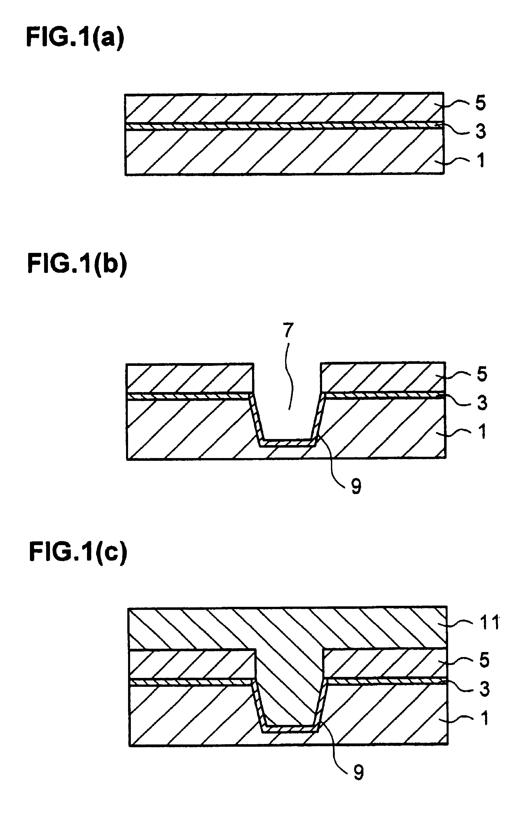
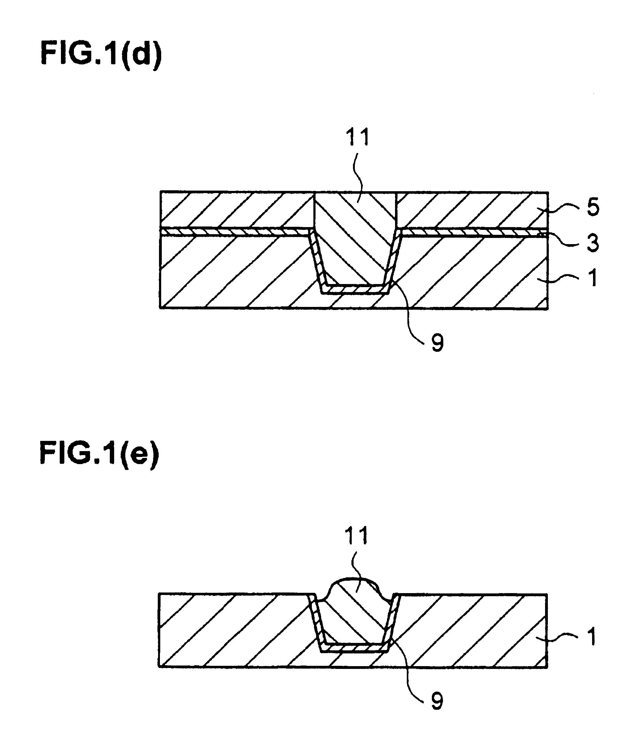
[0027]The following is a detailed explanation of the preferred embodiments of the present invention, given in reference to the drawings. FIG. 1 presents sectional views of the semiconductor device manufacturing steps in the present invention.[0028]1) First, as illustrated in FIG. 1(a), a pad oxide film 3 is formed to a thickness of 100-300 angstroms on an Si substrate 1 in a wet O2 atmosphere at 850 degrees centigrade. Over the pad oxide film 3 thus formed, an Si3N4 film 5 is formed to a thickness of 1500-2000 angstroms through LPCVD (low pressure CVD).[0029]2) Next, a photolithography process is performed and the Si3N4 film 5 is etched through the RIE (reactive ion etching) method. With a resist applied, the Si substrate 1 is etched by using the Si3N4 film 5 as a mask and the resist is removed to form a trench 7.[0030]3) As shown in FIG. 1(b), a trench liner oxide film 9 is formed to a thickness of 300 angstroms by employing the RTA (rapid thermal anneal) method in which oxidizing / ...

fifth embodiment

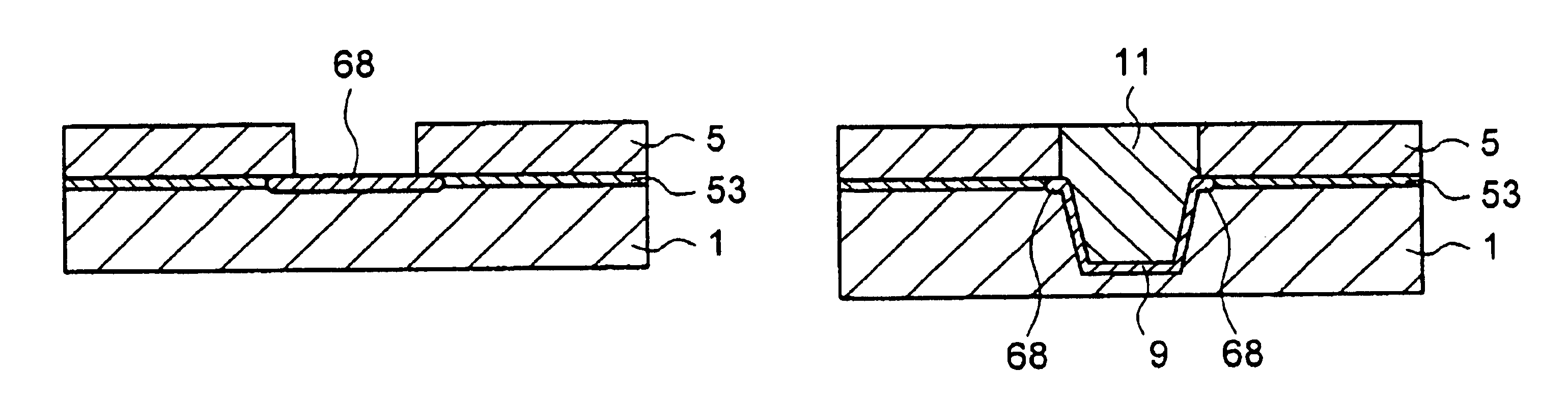
[0056]Next, the trench is filled with a CVD oxide film 11 and, as illustrated in FIG. 6(c), CMP is performed for planarization. As illustrated in FIG. 6(d), the S3N4 film 5 and the pad oxide film 53 are removed to form a field area. As shown in FIG. 6(e), a gate oxide film 48 is formed through oxidizing / nitriding as in the fifth embodiment, ion implementation is implemented to determine the transistor threshold voltage and activation annealing is performed. Then, specific steps are implemented to form a transistor.

[0057]During this process, the trench 7 may be formed after the sacrificial LOCOS 68 is formed by using the S3N4 film 5 as a mask without implementing the photolithography process. In such a case, since the photolithography process is skipped, the manufacturing method is simplified.

[0058]In this embodiment, since the remaining portion of the LOCOS 68 formed as a sacrifice constitutes an oxide film containing nitrogen, which acthieves a higher degree of HF resistance compar...


PUM


Abstract

The present invention provides a semiconductor device that reduces the junction leak current and achieves an improvement in the reliability of the gate oxide film by minimizing divot formation and the occurrence of a kink and a method of manufacturing such a semiconductor device. A pad oxide film and a silicon nitride film are formed on an Si substrate and a groove-like trench is formed through photolithography and etching. The liner oxide of the trench are oxidized through oxidizing / nitriding. Then, the trench is filled with an insulating film, the insulating film is planarized and the silicon nitride film and the pad oxide film are removed. Next, a field area is formed and a transistor is formed by following specific steps. By forming a trench liner oxide film containing nitrogen, stress is reduced.

Description

BACKGROUND OF THE INVENTION[0001]The present invention relates to a structure of an element isolation region in a semiconductor device and a semiconductor device manufacturing method.[0002]In a semiconductor device having silicon as its main constituent, an element isolation region (hereafter referred to as a field area) is formed through the LOCOS (local oxidation of silicon) method or the STI (shallow trench isolation) method to electrically isolate elements in the prior art. An area other than the field area is referred to as an active area, and the elements are formed in the active area. When a field area is formed through the LOCUS method, a bird's beak is formed at an end of the field area, reducing the size of the area that can be utilized as active area. With further miniaturization of elements achieved in recent years, the width and the pitch of the active area have become smaller and the use of the LOCOS method to form the field area is problematic. In contrast, the STI me...

Claims


Application Information

Patent Timeline
IPC IPC(8): H01L21/76H01L21/31H01L21/762
CPCH01L21/76235
Inventor YAMAUCHI, MICHIKO
Owner LAPIS SEMICON CO LTD
Why Eureka
Try Eureka