Electronic device manufacturing apparatus and method for manufacturing electronic device

a manufacturing apparatus and electronic device technology, applied in the field of electronic device manufacturing apparatus, can solve the problems of insufficient size of the reaction region of the electronic device manufacturing apparatus suitable for the field of giant microelectronics, inability to control the generation inability to realize the production of structurally complex plasma, etc., to achieve the effect of improving the mass-productivity of the electronic device, improving the quality, and reducing the reaction region

Inactive Publication Date: 2006-04-18
SHARP KK
View PDF14 Cites 1 Cited by
  • Summary
  • Abstract
  • Description
  • Claims
  • Application Information

AI Technical Summary

Benefits of technology

[0094]Thus, the invention described herein makes possible the advantages of: (1) providing an electronic device manufacturing apparatus in which the reaction region can be made larger even when a high frequency in the VHF range is used as a high frequency for plasma excitation power source, and which thus considerably improves the mass-productivity of electronic devices in the field of electronic industries such as those called “giant microelectronics” (which involves the manufacturing of solar batteries and liquid crystal display devices using an a-Si:H thin film, or photosensitive drums, etc.); (2) providing an electronic device manufacturing apparatus in which plasma damage (i.e., damage to a film or a substrate due to ion species in plasma) can be suppressed to a low level even under a high-speed deposition / etching condition, and which can thereby produce electronic devices with improved quality; and (3) providing a method for manufacturing an electronic device using such a manufacturing apparatus.

Problems solved by technology

Thus, so far, the reaction region of these apparatuses have not been made sufficiently large, and electronic device manufacturing apparatuses suitable for the field of electronic industries of giant microelectronics have not been realized.
Such a change results in generation of structurally complicated plasma which cannot be controlled.
It was thus confirmed that, due to the locationally-abnormal discharge, it is not possible, using the conventional plasma CVD apparatus 800 with a frequency in the VHF range, to cause electric discharge over a large area for large-area film deposition.
However, these techniques can only be applied to methods which aim to control plasma generation on the assumption that a high frequency in the RF range is used.
As these methods are applied to an electronic device manufacturing apparatus which uses a high frequency in the VHF range, the above-mentioned problems cannot be solved for the following reasons.
Therefore, it is not possible to control the value of the floating capacitance discussed above.
Furthermore, in accordance with the method described in Japanese Laid-Open Patent Application No. 6-61185, the impedance of the cathode electrode side cannot be controlled since the impedance adjusting element is provided on the side of the anode electrode.
However, since the size of the reaction region 83 is determined by the size of the substrate on which a film is deposited, it is practically difficult to vary the magnitude of the inductance LG of the reaction region 83.
Accordingly, it has not been possible to improve the mass-productivity of electronic devices.

Method used


Image

  • Electronic device manufacturing apparatus and method for manufacturing electronic device
  • Electronic device manufacturing apparatus and method for manufacturing electronic device
  • Electronic device manufacturing apparatus and method for manufacturing electronic device

Examples


example 1

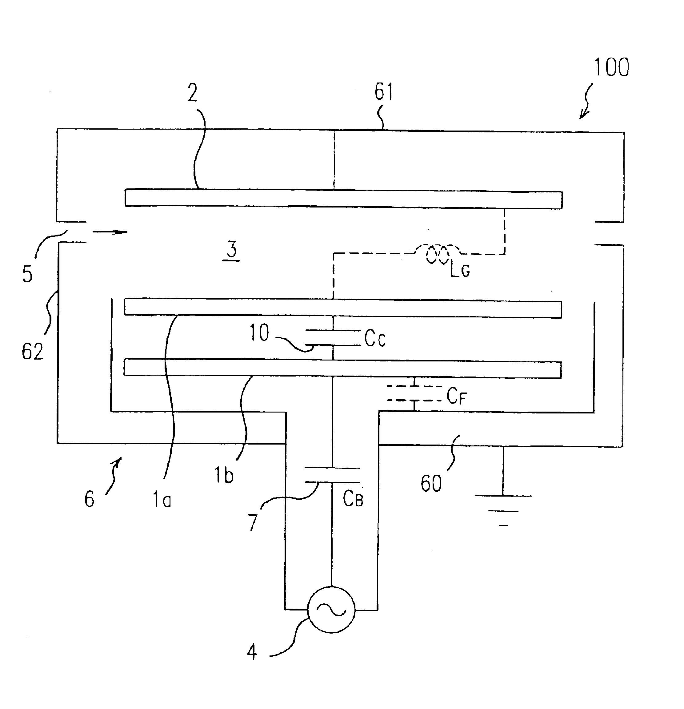
[0156]FIG. 1 illustrates an electronic device manufacturing apparatus 100 according to Example 1 of the present invention. The electronic device manufacturing apparatus 100 is implemented as a plasma CVD apparatus. The apparatus 100 includes a reaction chamber 6 which has a rectangular cross section. The anode electrode 2, the upper cathode electrode 1a and the lower cathode electrode 1b are provided within the reaction chamber 6. A bottom wall 60 of the reaction chamber 6 is grounded at some location in the right (in the figure) half thereof. The anode electrode 2 is electrically connected to an upper wall 61 of the reaction chamber 6, so as to be grounded.

[0157]The bottom wall 60 includes an opening in the middle of its length. The opening is insulated from the wall of the reaction chamber 6. A high frequency power generation source 4 is provided below the opening. The DC blocking capacitance element 7 (CB) formed of a capacitor is connected in series between the high frequency po...

example 2

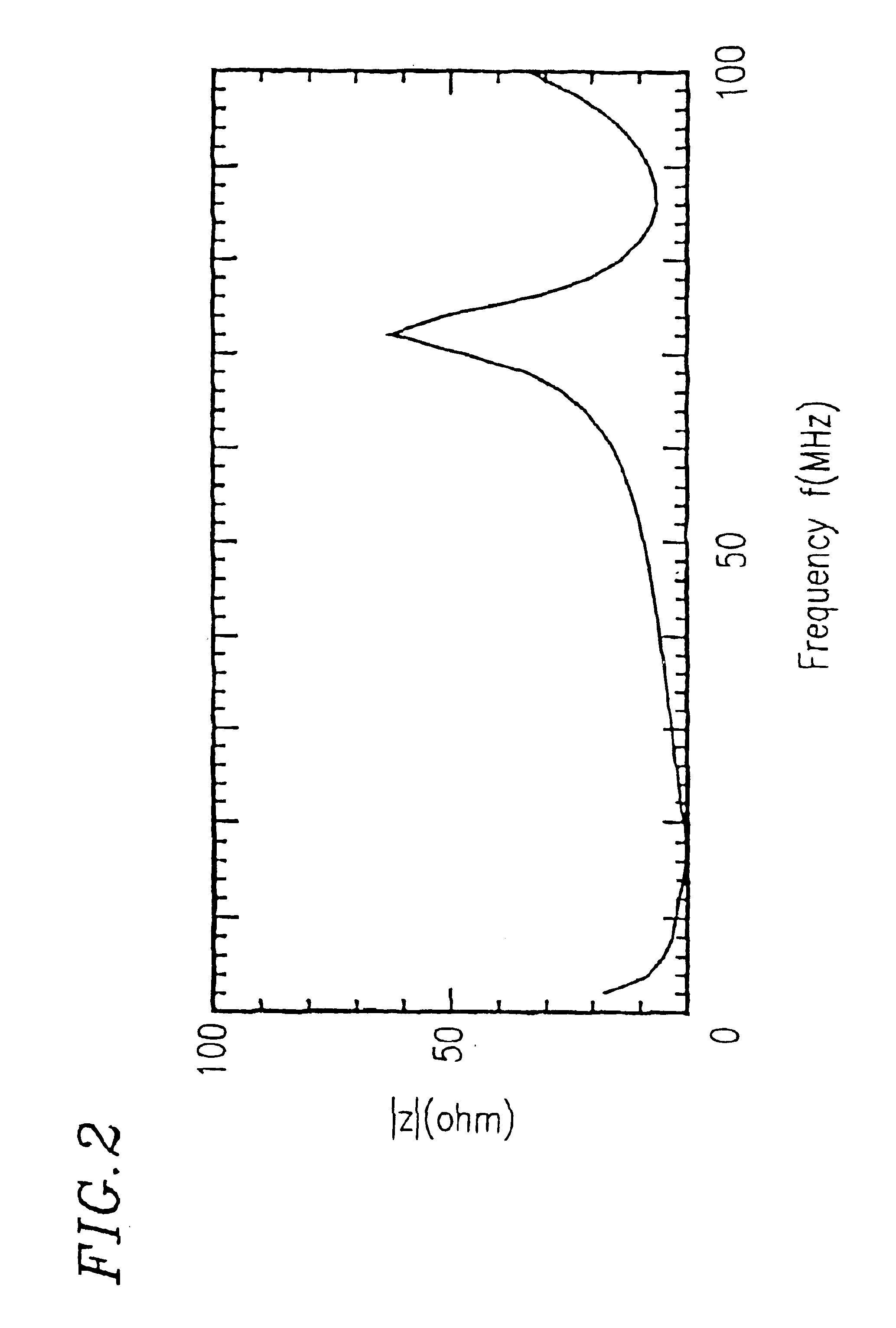
[0169]FIGS. 3 and 4 are provided for illustrating an electronic device manufacturing apparatus 200 according to Example 2 of the present invention. The electronic device manufacturing apparatus 200 of Example 2 is also implemented as a plasma CVD apparatus. The difference from Example 1 is in the element that serves as the impedance adjusting capacitor having capacitance value CC. In Example 1, a capacitor is inserted to form the impedance adjusting capacitance CC. In Example 2, as shown in FIG. 3, a dielectric 11 (e.g., having a thickness of about 50 mm and a relative dielectric constant of about 3.0) is inserted to form the impedance adjusting capacitance CC between the cathode electrodes 1a and 1b. Components of the apparatus 200 of Example 2 shown in FIG. 3 which are also provided in the apparatus 100 of Example 1 are denoted by the same reference numerals and will not be described in detail below.

[0170]FIG. 4 shows the frequency dependency of the magnitude |Z| of the impedance ...

example 3

[0172]FIG. 5 illustrates an electronic device manufacturing apparatus 300 according to Example 3 of the present invention. The electronic device manufacturing apparatus 300 of Example 3 is also implemented as a plasma CVD apparatus. The difference from Examples 1 and 2 is as follows. In Example 3, as shown in FIG. 5, the dielectric 11 is provided on the cathode electrode 11 so as to form the impedance adjusting capacitor 11 having a capacitance value CC, while the electrode corresponding to the upper cathode electrode 1a, as in Examples 1 and 2, is eliminated. Components of the apparatus 300 of Example 3 shown in FIG. 5 which are also provided in the apparatuses of Examples 1 and 2 are denoted by the same reference numerals.

[0173]Herein, the dielectric 11 is formed of teflon having a relative dielectric constant of about 2.0 and a thickness of about 35 mm, and provides an impedance adjusting capacitance CC of about 250 pF.

[0174]In this structure, electrons in the plasma generated in...


PUM

PropertyMeasurementUnit
excitation frequencyaaaaaaaaaa
lengthaaaaaaaaaa

Abstract

An electronic device manufacturing apparatus includes: a reaction chamber including a wall having a ground potential level; a reaction gas inlet for introducing a reaction gas into the reaction chamber; a high frequency power generator for generating a high frequency voltage for exciting the reaction gas into plasma state or dissociated state; a cathode electrode connected to the high frequency power generator; and a floating capacitance formed between a potential level of the cathode electrode and the ground potential level. An impedance adjusting capacitor is inserted so as to be in series with the floating capacitance. The impedance adjusting capacitor has a capacitance value less than that of the floating capacitance.

Description

BACKGROUND OF THE INVENTION[0001]1. Field of the Invention[0002]The present invention relates to an electronic device manufacturing apparatus. More particularly, the present invention relates to an electronic device manufacturing apparatus and a method for manufacturing an electronic device using such an apparatus, which are suitable for plasma excitation chemical vapor deposition (hereinafter, referred to as a “plasma CVD apparatus”) or for plasma etching. Plasma CVD apparatuses are used in electronic industries for producing a semiconductor film, such as an amorphous silicon hydride thin film (hereinafter, referred to as an “a-Si:H thin film”), or an insulating film. Plasma etching apparatuses are used for processing a semiconductor device, a liquid crystal device, and the like.[0003]2. Description of the Related Art[0004]Plasma CVD apparatuses are used to deposit a thin film through plasma excitation and plasma dissociation of a material gas. On the other hand, plasma dry etching...

Claims


Application Information

Patent Timeline
Patent Type & Authority Patents(United States)
IPC IPC(8): C23C16/509C23C16/50H05H1/46C23F4/00H01J37/32H01L21/205H01L21/302H01L21/3065H01L21/31
CPCC23C16/5096H01J37/32174
Inventor SAKAI, OSAMUNOMOTO, KATSUHIKO
Owner SHARP KK
Why Eureka
Try Eureka