
Apparatus and method for treating a substrate

a technology for treating apparatuses and substrates, applied in the direction of coatings, chemical vapor deposition coatings, metallic material coating processes, etc., can solve the problems of poor influence on mass productivity, difficult growth of phase-change layers, and inability to follow limitations, so as to prevent the deposition characteristics of phase-change layers and improve the mass-productivity of phase-change memories. , the effect of preventing the incubation time and directivity of phase-change layers

Active Publication Date: 2015-02-05
WONIK IPS CO LTD
View PDF13 Cites 1 Cited by
  • Summary
  • Abstract
  • Description
  • Claims
  • Application Information

AI Technical Summary

Benefits of technology

The present invention provides an apparatus and method for depositing a phase-change memory on a substrate. The invention prevents changes in the deposition characteristics of the phase-change layer caused by a plasma cleaning process on the bottom electrode. It also prevents variations in the incubation time and direction of the phase-change layer caused by the plasma cleaning process. Additionally, the invention improves mass-productivity of the phase-change memory.

Problems solved by technology

However, it may be difficult to grow a phase-change layer that is the high quality GST thin film at a low temperature through the CVD and ALD.
Particularly, when the phase-change layer is deposited after a bottom electrode is formed, following limitations may occur.
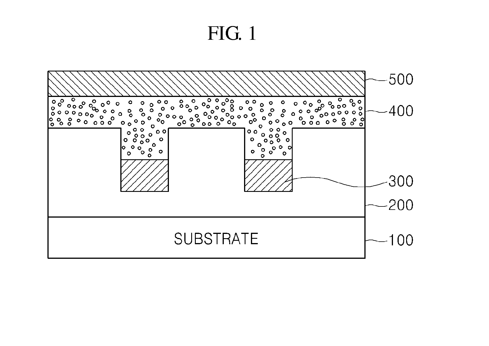
That is, deposition characteristics of the phase-change layer 400 due to the bonding of the hydrogen H on the surfaces of the thin films may be changed to significantly affect an incubation time and directivity, thereby having a bad influence on mass productivity.

Method used


Image

  • Apparatus and method for treating a substrate
  • Apparatus and method for treating a substrate
  • Apparatus and method for treating a substrate

Examples


Embodiment Construction

[0032]Hereinafter, specific embodiments will be described in detail with reference to the accompanying drawings. The present disclosure may, however, be embodied in different forms and should not be construed as limited to the embodiments set forth herein. Rather, these embodiments are provided so that this disclosure will be thorough and complete, and will fully convey the scope of the present disclosure to those skilled in the art. In the figures, like reference numerals refer to like elements throughout.

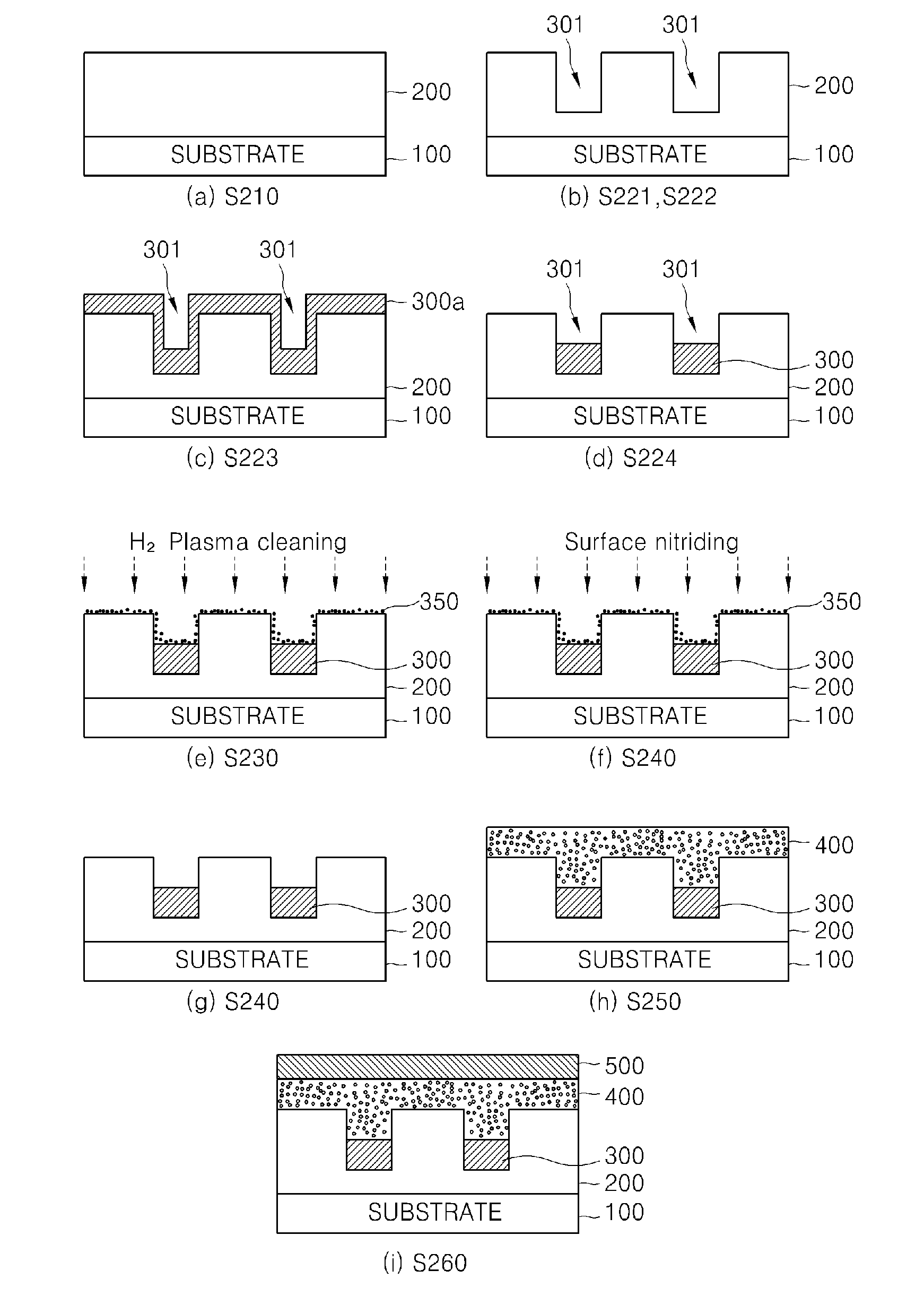
[0033]FIG. 2 is a flowchart illustrating a process of depositing a PRAM material in accordance with an exemplary embodiment, and FIG. 3 is a view illustrating a process of depositing the PRAM material in accordance with an exemplary embodiment.

[0034]A phase-change RAM (PRAM) includes a phase-change layer that be changed in crystalline state according to heat generated from applied current. At present, a chalcogenide compound (GST: Ge-Sb-Te) including germanium (Ge), antimony (Sb),...


PUM

PropertyMeasurementUnit
temperatureaaaaaaaaaa
sizeaaaaaaaaaa

Abstract

Provided are a substrate treating apparatus and method of manufacturing a phase-change layer having superior deposition characteristics. The substrate treating method of manufacturing a phase-change memory includes forming a bottom electrode on a substrate on which a pattern is formed, performing surface treating for removing impurities generated or remaining on a surface of the substrate while the bottom electrode is formed, performing nitriding on the surface of the substrate from which the impurities are removed, and successively depositing a phase-change layer and a top electrode on the bottom electrode. The substrate treating apparatus for manufacturing a phase-change memory includes a load lock chamber into / from which a plurality of substrates are loaded or unloaded, the load lock chamber being converted between an atmosphere state and a vacuum state, a nitriding chamber in which nitriding is performed on a surface of a substrate on which a bottom electrode is disposed, the nitriding chamber being coupled to one side of a plurality of sides of the vacuum transfer chamber, and a process chamber in which a phase-change layer is deposited on the surface of the substrate on which nitriding is performed in the nitriding process chamber, the process chamber being coupled to one of the plurality of sides of the vacuum transfer chamber.

Description

CROSS-REFERENCE TO RELATED APPLICATION[0001]This application claims priority to Korean Patent Application No. 10-2011-0112128 filed on Oct. 31, 2011 and all the benefits accruing therefrom under 35 U.S.C. §119, the contents of which are incorporated by reference in their entirety.BACKGROUND[0002]The present disclosure relates to a substrate treating apparatus for depositing a phase-change layer of a phase change random access memory (PRAM) and a substrate treating method, and more particularly, to a substrate treating apparatus and method for manufacturing a phase-change layer having superior deposition characteristics.[0003]The next generation non-volatile memories for supplementing faults of existing non-volatile memories such as dynamic random access memories (DRAMs), static random access memories (SRAMs), and flash memories are being proposed. Ferroelectrics random access memories (FRAMs), magnetic random access memories (MRAMs), phase-change random access memories (PRAMs), and ...

Claims


Application Information

Patent Timeline
Patent Type & Authority Applications(United States)
IPC IPC(8): H01L45/00C23C16/52C23C16/50H10B69/00
CPCH01L45/1616H01L45/1253C23C16/52H01L45/144C23C16/50H01L45/06H10N70/231H10N70/8825H10N70/826H10N70/884H10N70/8828H10N70/023H10N70/011H10N70/066H10N70/841
Inventor PARK, JU HWANRYU, DONG HOCHO, BYUNG CHUL
Owner WONIK IPS CO LTD
Learn More