
White light emitting structures with controllable emission color temperature

a technology of white light and color temperature, which is applied in the direction of lasers, semiconductor laser arrangements, semiconductor lasers, etc., can solve the problems of nonpolar templates, affecting the device performance, and the mqw active region of electrically pumped devices

Active Publication Date: 2018-05-29
OSTENDO TECH INC
View PDF70 Cites 10 Cited by
  • Summary
  • Abstract
  • Description
  • Claims
  • Application Information

AI Technical Summary

Benefits of technology

The patent text discusses methods for controlling the distribution of charge carriers in multi-layer active regions of electrically pumped solid state light emitters such as light-emitting diodes and laser diodes. The technical effect of the patent is to improve the performance of these devices by tailoring and controlling the distribution of charge carriers to decrease optical and electrical losses, minimize strain relaxation length, and reduce the impact of non-uniform carrier injection on device performance. The patent references several conventional methods and proposes new approaches to achieve multi-color emission and high carrier injection efficiency.

Problems solved by technology

On the other hand, MQW active regions of electrically pumped devices typically suffer from inhomogeneous distribution of charge carriers, both electrons and holes, which are injected from the opposite sides of the diode structure.
As a result, uneven and imbalanced population of active QWs unfavorably affects the device performance.
Nonpolar templates, however, do not solve the problem of inhomogeneous injection entirely.
Even in the absence of internal polarization fields, MQW structures with sufficiently deep QWs and strong carrier confinement reveal uneven QW populations in a wide range of injection currents, so that the carrier population non-uniformity in III-nitride MQWs is a common feature of both polar and non-polar templates.

Method used


Image

  • White light emitting structures with controllable emission color temperature
  • White light emitting structures with controllable emission color temperature
  • White light emitting structures with controllable emission color temperature

Examples


Embodiment Construction

[0027]Various embodiments and aspects of the disclosure herein will be described with reference to details discussed below, and the accompanying figures will illustrate the various embodiments. The following description and figures are illustrative of the disclosure herein and are not to be construed as limiting. Numerous specific details are described to provide a thorough understanding of various embodiments. However, it is understood that embodiments disclosed herein may be practiced without these specific details. In certain instances, well-known or conventional details, such as circuits, structures, and techniques, are not described in order to provide a concise discussion of example embodiments.

[0028]Reference in the specification to “one embodiment” or “an embodiment” means that a particular feature, structure, or characteristic described in conjunction with the embodiment can be included in at least one embodiment of the invention. The appearances of the phrase “in one embod...


PUM


Abstract

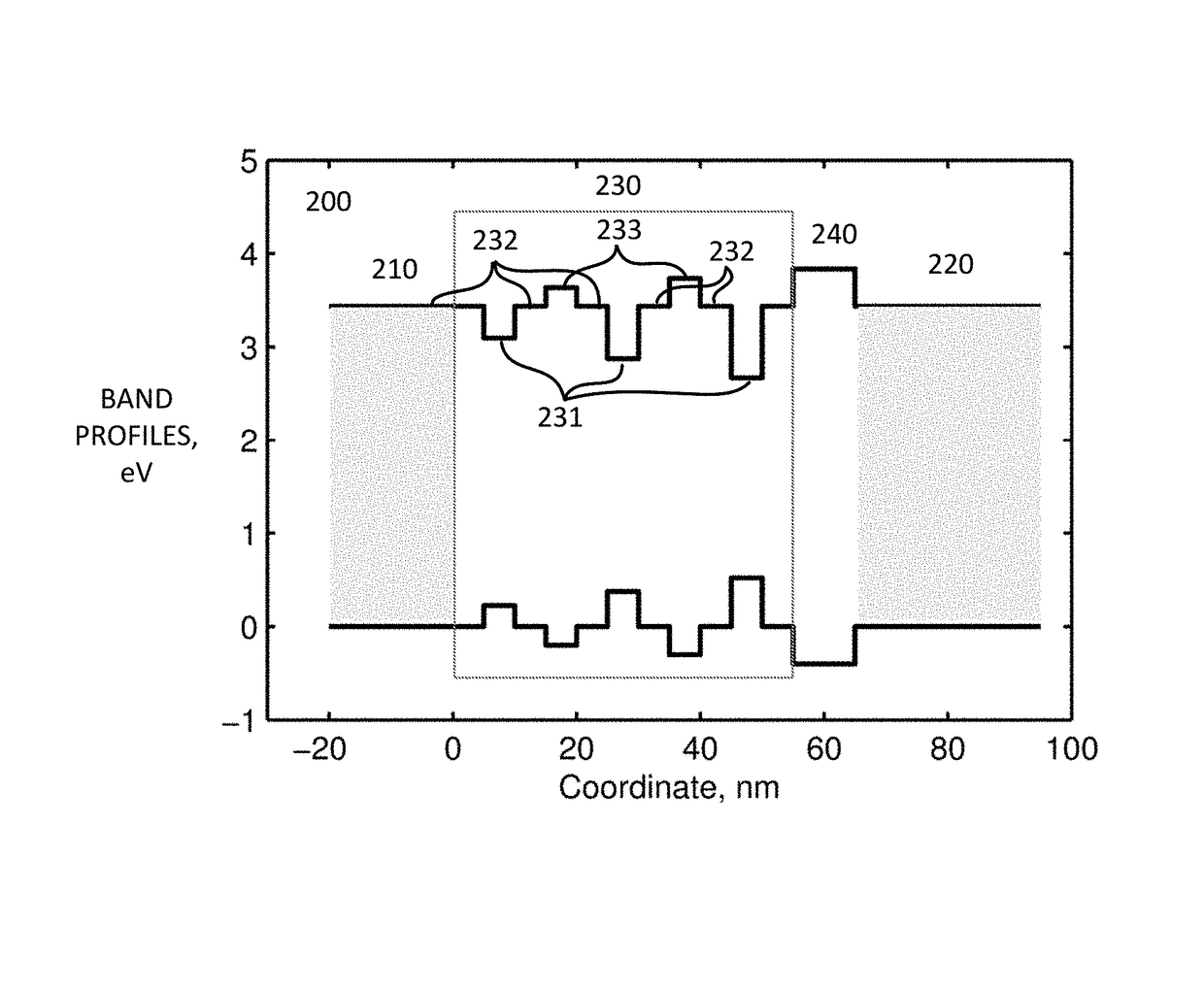
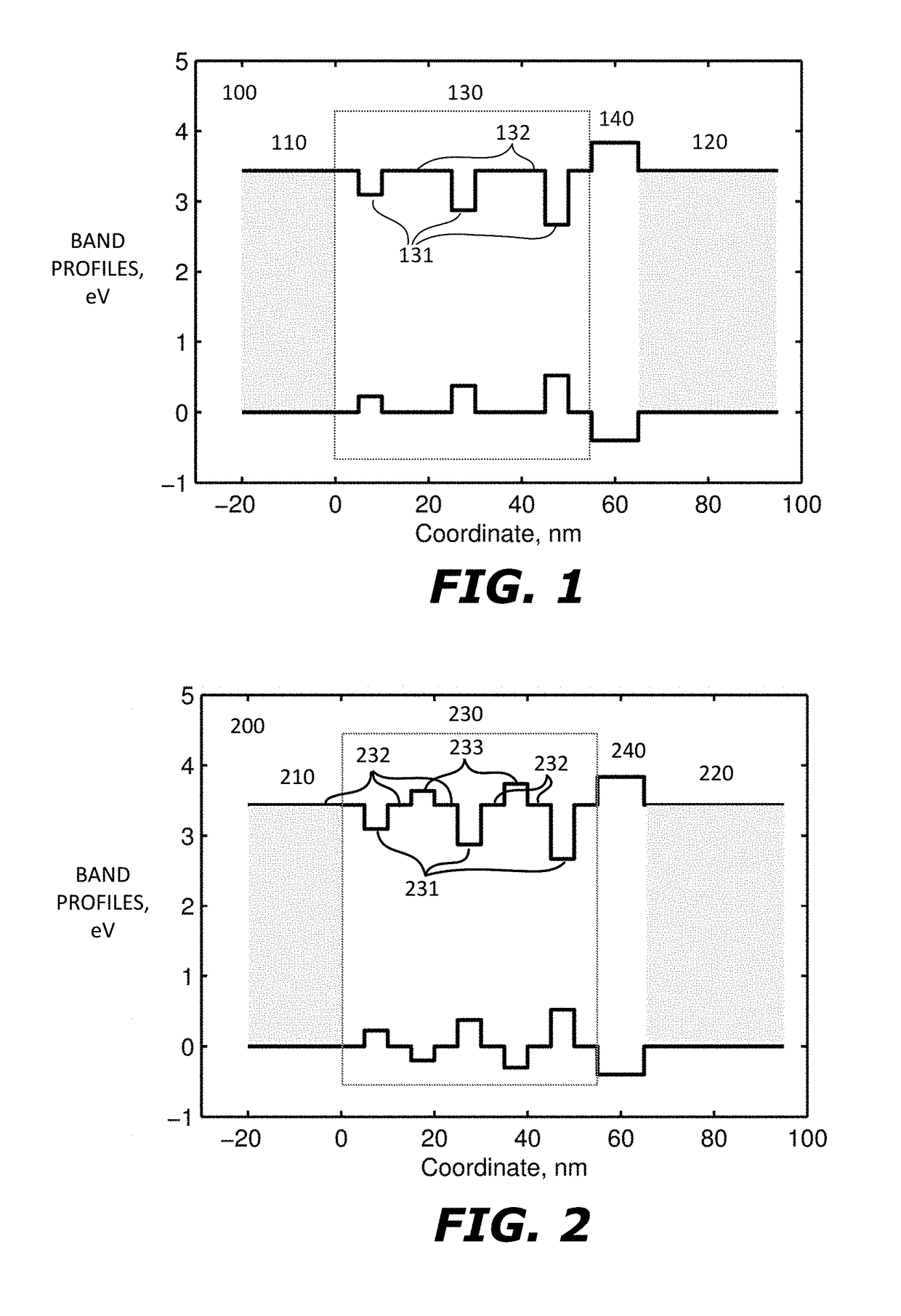
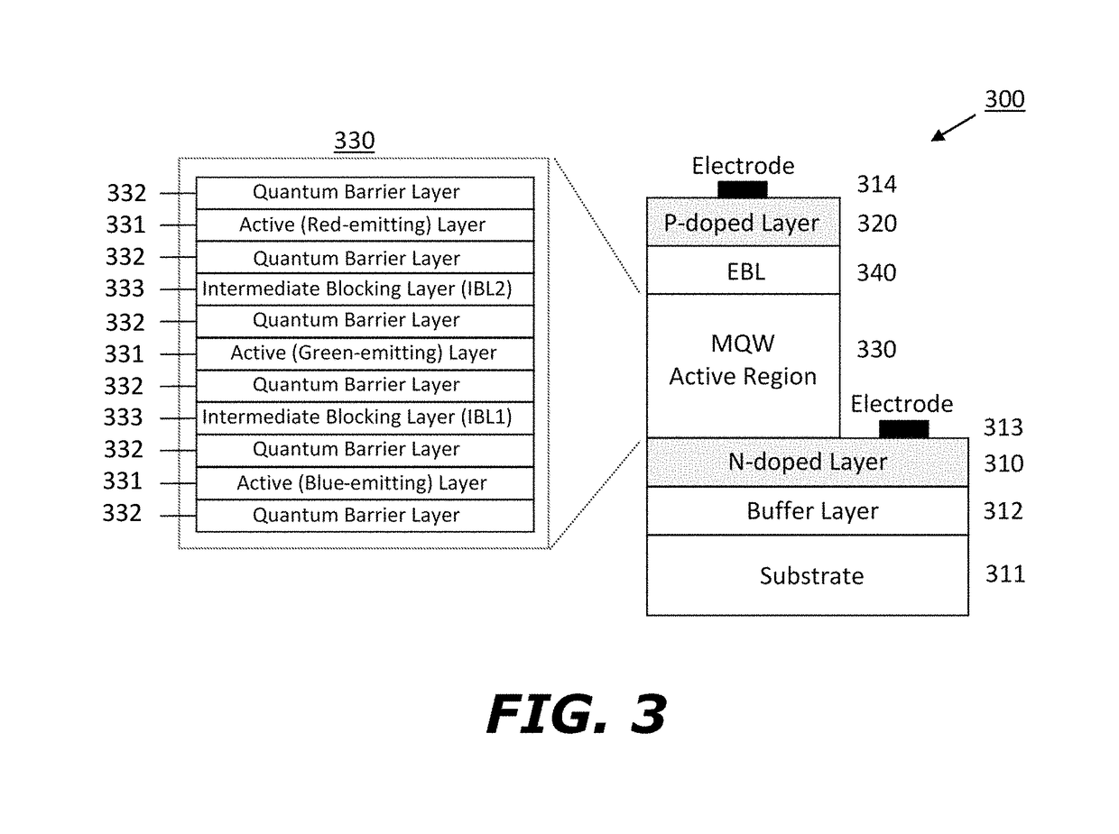
Disclosed herein are multi-layered optically active regions for semiconductor light-emitting devices (LEDs) that incorporate intermediate carrier blocking layers, the intermediate carrier blocking layers having design parameters for compositions and doping levels selected to provide efficient control over the carrier injection distribution across the active regions to achieve desired device injection characteristics. Examples of embodiments discussed herein include, among others: a multiple-quantum-well variable-color LED operating in visible optical range with full coverage of RGB gamut, a multiple-quantum-well variable-color LED operating in visible optical range with an extended color gamut beyond standard RGB gamut, a multiple-quantum-well light-white emitting LED with variable color temperature, and a multiple-quantum-well LED with uniformly populated active layers.

Description

CROSS-REFERENCE TO RELATED APPLICATIONS[0001]This application claims the benefit of U.S. Provisional Patent Application No. 62 / 171,536, filed Jun. 5, 2015, U.S. Provisional Patent Application No. 62 / 275,650, filed Jan. 6, 2016, and U.S. Provisional Patent Application No. 62 / 290,607, filed Feb. 3, 2016, the contents of each of which are hereby incorporated by reference as if fully stated herein.FIELD OF THE INVENTION[0002]The disclosure herein relates to means for tailoring and controlling the distribution of charge carriers in multi-layer active regions of electrically pumped solid state light emitters such as light-emitting diodes and laser diodes.BACKGROUND OF THE INVENTION[0003]Semiconductor light emitting diode structures have become the established leaders among optical light sources in different emission wavelength ranges. A conventional light-emitting structure is typically comprised of multiple layers of III-V compound semiconductor alloys such as GaAsP, AlGaAs, AlGaInP, or ...

Claims


Application Information

Patent Timeline
Patent Type & Authority Patents(United States)
IPC IPC(8): H01L27/15H01L33/08H01S5/343H01S5/042H01L33/32H01L33/06H01L33/00H01S5/34H01S5/10H01S5/40H01S5/20
CPCH01L33/08H01L33/06H01L33/32H01S5/0421H01S5/34333H01S5/4093H01S5/1096H01S5/2009H01S5/3407H01S5/4043H01L33/145H01L33/12H01S5/0622
Inventor EL-GHOROURY, HUSSEIN S.KISIN, MIKHAIL V.YEH, YEA-CHUAN MILTONCHUANG, CHIH-LICHEN, JYH-CHIA
Owner OSTENDO TECH INC
Learn More