Ultra small and ultrathin high luminous efficiency lateral emission type high light white light polycrystalline LED element
A high-efficiency, LED chip technology, used in electrical components, electrical solid-state devices, semiconductor devices, etc., can solve the problems of insufficiency, large size, inability to miniaturize, etc., to reduce product size, improve heat dissipation, and save space. Effect
- Summary
- Abstract
- Description
- Claims
- Application Information
AI Technical Summary
Problems solved by technology
Method used
Image

Examples
Embodiment 1
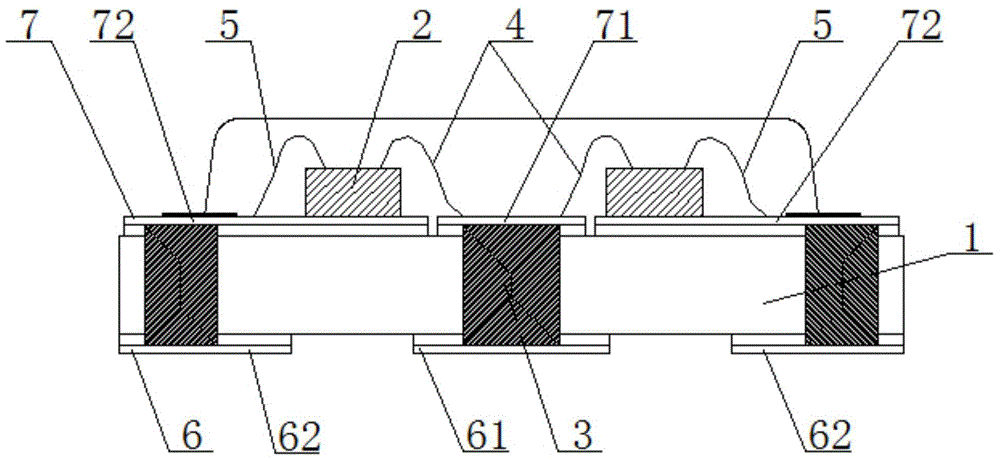
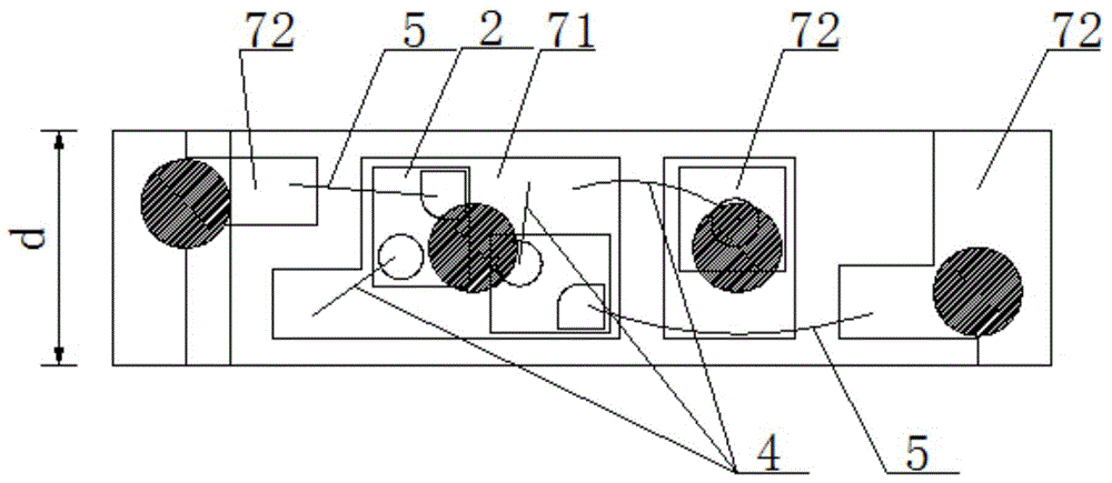
[0036] Preferred embodiment one: as figure 1 There are two light-emitting LED chips 2 shown, and the positive wires 4 of the two light-emitting LED chips 2 are welded to the positive region 71 in the middle, and the two negative wires 5 are respectively connected to two mutually independent negative regions 72 on both sides. welding. The ultra-small, ultra-thin, high-efficiency side-firing high-brightness white light twin-crystal LED element is rectangular: its length is 1.6±0.2mm, its width is 0.6±0.2mm, and its thickness d is 0.3±0.1mm. Preferably: length 1.6mm, width 0.6mm, thickness 0.3mm.
Embodiment 2
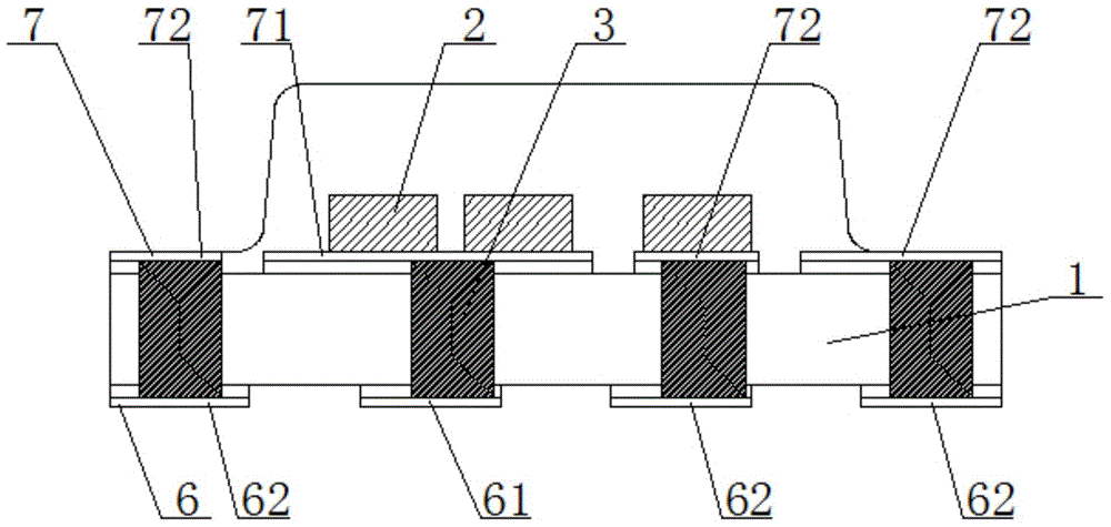
[0037] Preferred embodiment two: as figure 2 , 3 There are three light-emitting LED chips 2 shown, and the positive wires 4 of the three light-emitting LED chips 2 are all welded to the positive region 71 in the middle, and the three negative wires 5 are respectively welded to three mutually independent negative regions 72 on both sides. . The ultra-small, ultra-thin, high-efficiency side-firing high-brightness white three-crystal LED element is rectangular: its length is 1.6±0.2mm, its width is 0.6±0.2mm, and its thickness d is 0.4±0.1mm. Preferably: length 1.6mm, width 0.6mm, thickness 0.4mm.
[0038] A process for preparing an ultra-small, ultra-thin, high-efficiency side-firing high-brightness white polycrystalline LED element, the steps are as follows:
[0039] a. Prepare raw materials: Drill through holes on the PCB substrate 1 and conduct the upper and lower bottom surfaces of the PCB substrate 1 through the copper plugging process to form the plug hole copper pilla...
PUM
 Abstract
Description
Claims
Application Information
 - Generate Ideas
- Intellectual Property
- Life Sciences
- Materials
- Tech Scout
- Unparalleled Data Quality
- Higher Quality Content
- 60% Fewer Hallucinations
Browse by: Latest US Patents, China's latest patents, Technical Efficacy Thesaurus, Application Domain, Technology Topic, Popular Technical Reports.
© 2025 PatSnap. All rights reserved.Legal|Privacy policy|Modern Slavery Act Transparency Statement|Sitemap|About US| Contact US: help@patsnap.com