
Super junction field effect transistor with internal floating ring

a technology of super junction field and transistor, applied in the direction of basic electric elements, electrical equipment, semiconductor devices, etc., can solve the problems of p-type columns with p-type charges that are not balanced along edges and corners

Active Publication Date: 2017-03-07
LITTELFUSE INC
View PDF9 Cites 0 Cited by
  • Summary
  • Abstract
  • Description
  • Claims
  • Application Information

AI Technical Summary

Benefits of technology

The patent text talks about a device called a floating ring-shaped P-type column that helps to increase the device's avalanche breakdown voltage, which is a measure of its resistance to damage. This is achieved by reducing the electric field along the upper surface of the floating ring-shaped column, which prevents maximum impact ionization during avalanche breakdown in nearby regions. The use of the floating ring-shaped column also makes the device less susceptible to process variations during fabrication, resulting in a more robust device.

Problems solved by technology

Such process variations may cause a charge imbalance along edges and corners along the P− type columns of the internal active area.

Method used


Image

  • Super junction field effect transistor with internal floating ring
  • Super junction field effect transistor with internal floating ring
  • Super junction field effect transistor with internal floating ring

Examples


Embodiment Construction

[0027]Reference will now be made in detail to some embodiments of the invention, examples of which are illustrated in the accompanying drawings. In the text and drawings, the dopant labels N++, N+, N−, N, P+, P−, and P are only very loose general descriptions of relative dopant concentrations. A particular dopant label appearing in the text below has meaning within the local context of its usage. In the text and drawings, the term P type is sometimes used not as a description of a relative dopant concentration, but rather is used as a broad term to denote semiconductor material that may be P− type, or may be P type, or may be P+ type, or that may include sub-regions of various P type dopant concentrations.

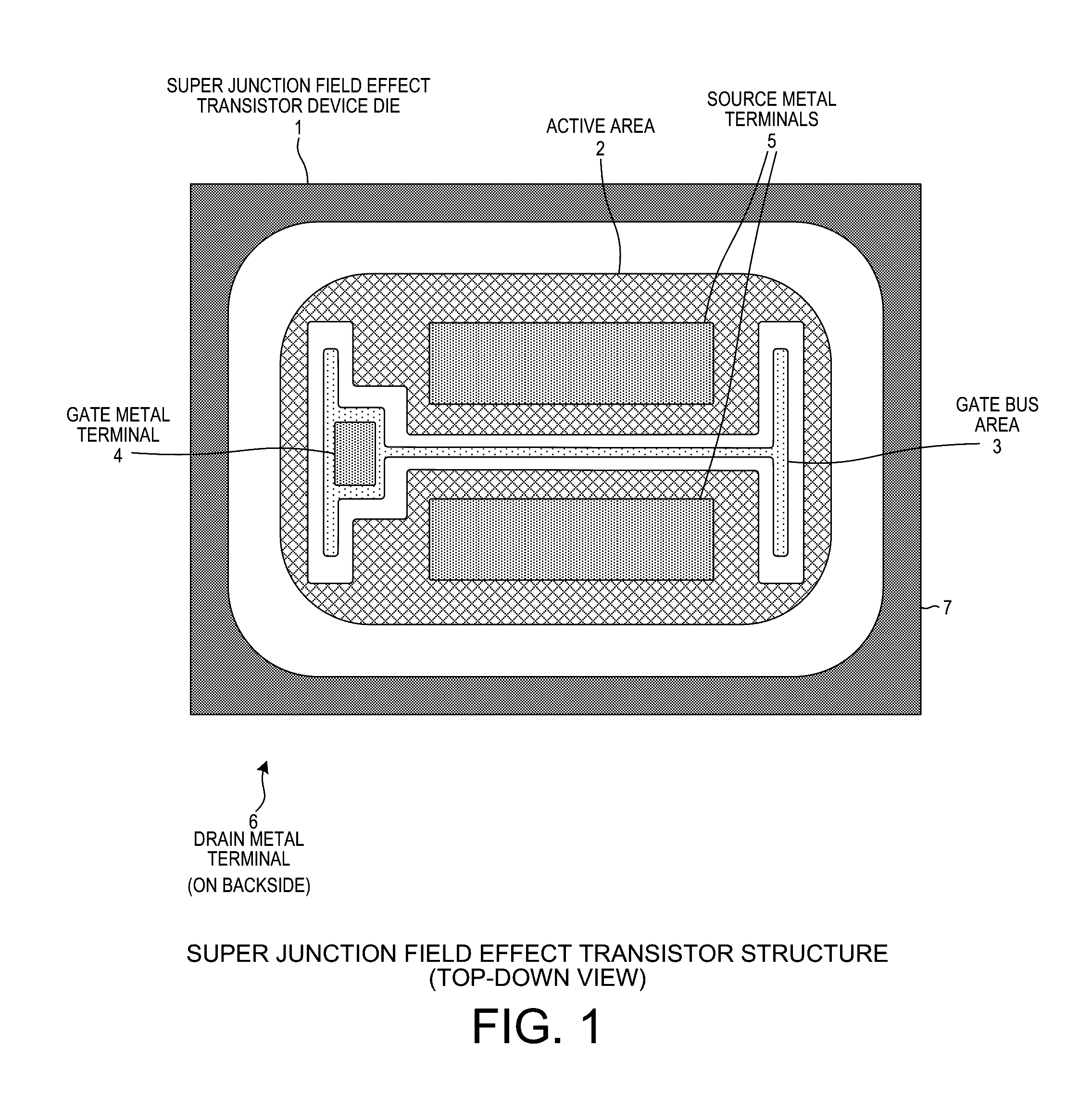
[0028]FIG. 1 is a top-down diagram of a Super Junction Field Effect Transistor (FET) device die 1 in accordance with one novel aspect. Such a Super Junction FET device die 1 is also loosely referred to as a Super Junction Metal Oxide Semiconductor Field Effect Transistor (MOSFET). ...


PUM


Abstract

A Super Junction Field Effect Transistor (FET) device includes a charge compensation region disposed on a substrate of semiconductor material. The charge compensation region includes a set of strip-shaped P− type columns, a floating ring-shaped P− type column that surrounds the set of strip-shaped P− type columns, and a set of ring-shaped P− type columns that surrounds the floating ring-shaped P− type column. A source metal is disposed above portions of the charge compensation region. The source metal contacts each of the strip-shaped P− type columns and each of the ring-shaped P− type columns. An oxide is disposed between the floating P− type column and the source metal such that the floating P− type column is electrically isolated from the source metal. The device exhibits a breakdown voltage that is 0.2% greater than if the floating P− type column were to contact the source metal.

Description

TECHNICAL FIELD[0001]The described embodiments relate generally to Super Junction field effect transistors and techniques for making rugged Super Junction field effect transistors.BACKGROUND INFORMATION[0002]Super junction techniques are often employed to fabricate an N-channel field effect transistor device. Such an N-channel field effect transistor device can be made whose drift region includes what is called a “charge compensation region”. The N-channel field effect transistor device is typically made to meet a particular breakdown voltage requirement. During fabrication, if the concentration of N-type dopants within the charge compensation region becomes undesirably imbalanced with respect to the concentration of P-type dopants within the charge compensation region, then the breakdown voltage requirement will not be satisfied. To maintain charge balance between the concentration of P-type dopants and N-type dopants, very tight process control is required. Fabricating the N-chann...

Claims


Application Information

Patent Timeline
Patent Type & Authority Patents(United States)
IPC IPC(8): H01L29/78H01L29/06H01L29/66H01L29/40
CPCH01L29/7811H01L29/0619H01L29/0634H01L29/0692H01L29/66712H01L29/402
Inventor SEOK, KYOUNG WOOK
Owner LITTELFUSE INC
Learn More