Power electronic semiconductor device

Pending Publication Date: 2021-11-23
威星国际半导体深圳有限公司
View PDF7 Cites 0 Cited by
  • Summary
  • Abstract
  • Description
  • Claims
  • Application Information

AI Technical Summary

Problems solved by technology

However, when this IGBT is turned on, there will be a lot of noise caused by electromagnetic interference EMI (Electro-MagneticInterference)

Method used


Image

  • Power electronic semiconductor device
  • Power electronic semiconductor device
  • Power electronic semiconductor device

Examples


Embodiment Construction

[0026] In order to express the present invention more clearly, the present invention will be further described below in conjunction with the accompanying drawings.

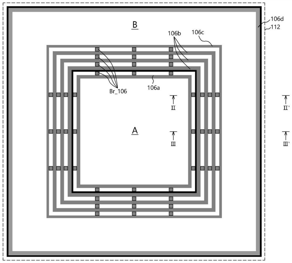
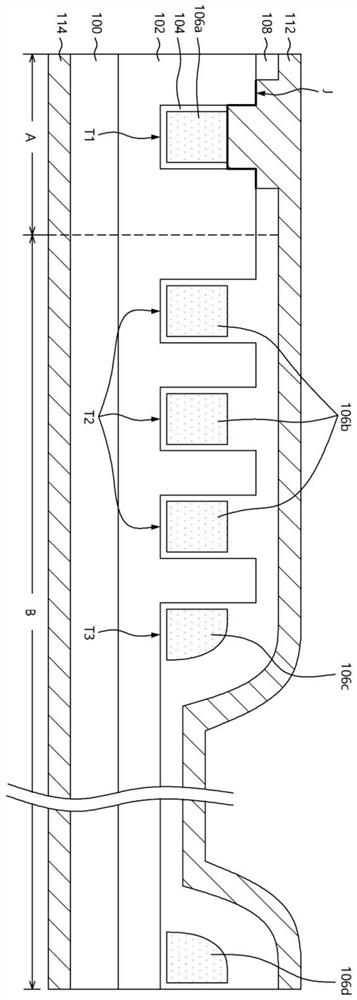
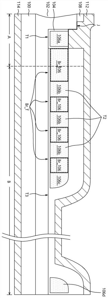
[0027] see Figure 1 to Figure 3 , the invention discloses a power electronic semiconductor device, comprising a semiconductor substrate, an active region and a junction termination region are arranged on the semiconductor substrate; a first trench is arranged in the active region, and a second trench is arranged at the junction of the active region and the junction termination region. Two grooves, a third groove is arranged in the junction terminal region; a Schottky diode semiconductor layer is arranged in the first groove; an electric field protection ring is arranged in the second groove, and a conductive space is arranged in the third groove The charge layer, the first groove, the second groove and the third groove are connected by Schottky diodes. The width of the first groove is the same as that of the sec...


PUM


Abstract

The invention discloses a power electronic semiconductor device, which comprises a semiconductor substrate, and is characterized in that the semiconductor substrate is provided with an active region and a junction terminal region; a first groove is formed in the active region, a second groove is formed in the joint of the active region and the junction termination region, and a third groove is formed in the junction termination region; a Schottky diode semiconductor layer is arranged in the first groove; an electric field protection ring is arranged in the second groove, a conductive space charge layer is arranged in the third groove, and the first groove, the second groove and the third groove are connected through a Schottky diode. A protection ring is formed on the interface of the Schottky diode semiconductor layer, the active area and the junction terminal area and is connected with a residual conductive space charge layer on the side face of the junction terminal area through a bridge to form an electric loop, so that the situation that an electric field in a semiconductor is reduced after a leakage current source and part of voltage are balanced is prevented, and the avalanche breakdown voltage is improved.

Description

technical field [0001] The present invention relates to the field of semiconductor devices, in particular to a power electronic semiconductor device. Background technique [0002] In order to achieve continuous reduction in consumption cost and increase in capacity of power conversion devices, power electronic semiconductor devices are expected to play a key role in energy saving and increase in capacity in power conversion devices. In order to make the on-state voltage lower, that is, the on-resistance lower, it is an optimal choice to use a transistor controlled by an insulated gate, that is, an IGBT (Insulated Gate Bipolar Transistor) device. Due to the use of IGBTs, a high breakdown voltage is ensured and a fast switching speed is achieved. However, when this IGBT is turned on, there will be a lot of noise caused by electromagnetic interference EMI (Electro-Magnetic Interference). Contents of the invention [0003] In order to solve the problem of electromagnetic int...

Claims


Application Information

Patent Timeline
Patent Type & Authority Applications(China)
IPC IPC(8): H01L27/06
CPCH01L27/06
Inventor 张涵张昌利金镇亨
Owner 威星国际半导体深圳有限公司
Why Eureka
Try Eureka