Universal surface-mount semiconductor package

a semiconductor and surface mount technology, applied in semiconductor devices, semiconductor/solid-state device details, electrical apparatus, etc., can solve the problems of imperfect mechanical processes, unavoidable variability, and inability to miniaturize in parts, so as to avoid the difficulties inherent in the bending of leads to form gull-wing packages, and without undue delay

Active Publication Date: 2017-02-21
ADVENTIVE INT LTD
View PDF10 Cites 11 Cited by
  • Summary
  • Abstract
  • Description
  • Claims
  • Application Information

AI Technical Summary

Benefits of technology

[0049]Leadless packages offer unique advantages in flexible package manufacturing, coplanarity, low-profile capability, and the elimination of the need for expensive package-specific mold cavity tools. For all of its advantages, one major disadvantage of the QFN / DFN leadless package is its inability to be used in wave-solder PCB factories. Because no metal lead protrudes laterally from the package, wave-soldering cannot penetrate beneath the package to solder the die pad and the conductive landings onto the PCB conductors. Instead, the solder must be screened using a mask onto the PCB before component placement. Also, solder flow must be performed in expensive reflow ovens or belt furnaces making the entire PCB assembly process 2 to 4 times more expensive than that of simple wave-solder factory based production. Moreover, visual inspection of leadless packages soldered to a PCB using simple automated camera inspection is impossible because the solder cannot be confirmed from the top view. Instead expensive X-ray inspection equipment is required, adding cost and safety risk into reflow PCB manufacturing.
[0056]What is needed is a single package design and manufacturing process that is able to produce surface-mount packages flexibly for both wave-solder and reflow assembly, facilitate superior coplanarity among the die pad and conductive leads, achieve low package height, provide good thermal power dissipation, minimize package inductance, and eliminate the need for package specific equipment such as mold cavity tools and leading equipment.SUMMARY OF THE INVENTION
[0069]Preferably, the wavelength and other characteristics of the first laser beam will be such that the first laser beam does minimal damage to the metal conductors embedded in or underlying the plastic block.
[0071]The techniques of this invention thus allow a wide variety of different types and sizes of semiconductor packages to be fabricated without the need for specialized equipment. This is attained by essentially varying the patterns of openings in the mask layers applied to the backside and front side surfaces of a metal sheet and by varying the combined width of the laser scans used to separate the plastic block into capsules for each package. Where footed packages are used, the bottom surfaces of the feet are assured of being coplanar, and the difficulties inherent in the bending of leads to form gull-wing packages are avoided.
[0072]As a result, a semiconductor package manufacturer can produce packages designed to meet its customers' specific needs economically and without undue delays.

Problems solved by technology

Unfortunately, mechanical processes are imperfect and subject to unavoidable variability.
As such, gull wing packages are not able to serve the market for thin products and such packages have been completely eliminated from cell phone and tablet designs.
Other products where gull wing packages persist because of their relatively low cost are, however, unable to be miniaturized in part because of the minimum height restrictions of gull wing packages.
Aside from issues with scaling gull wing packages to below 0.8 mm for low profile applications, such IC packages do not normally include a thick exposed die pad to act as a heat sink and without special design modifications are therefore unable to dissipate any significant power or spread heat effectively.
Unfortunately, 
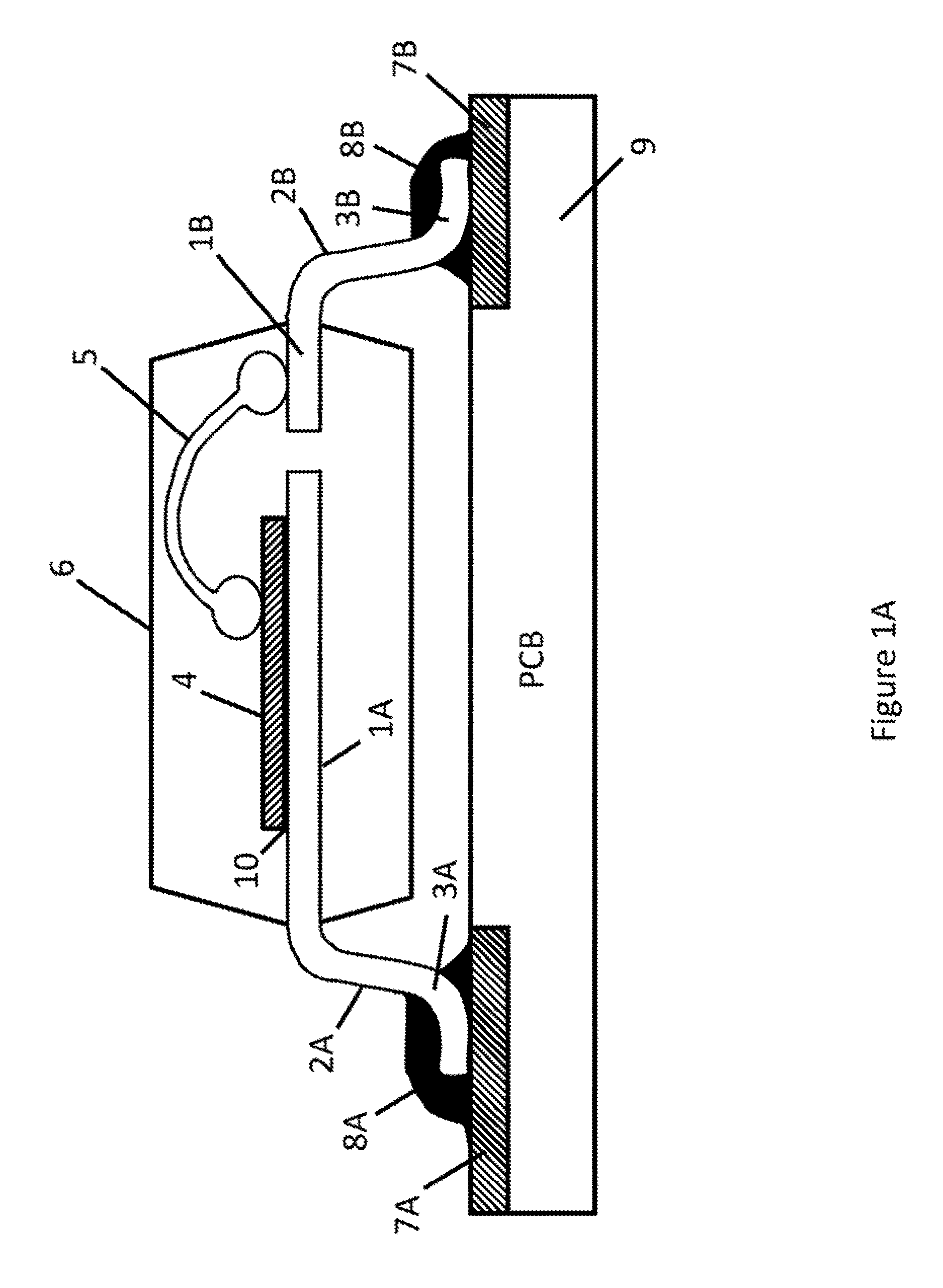
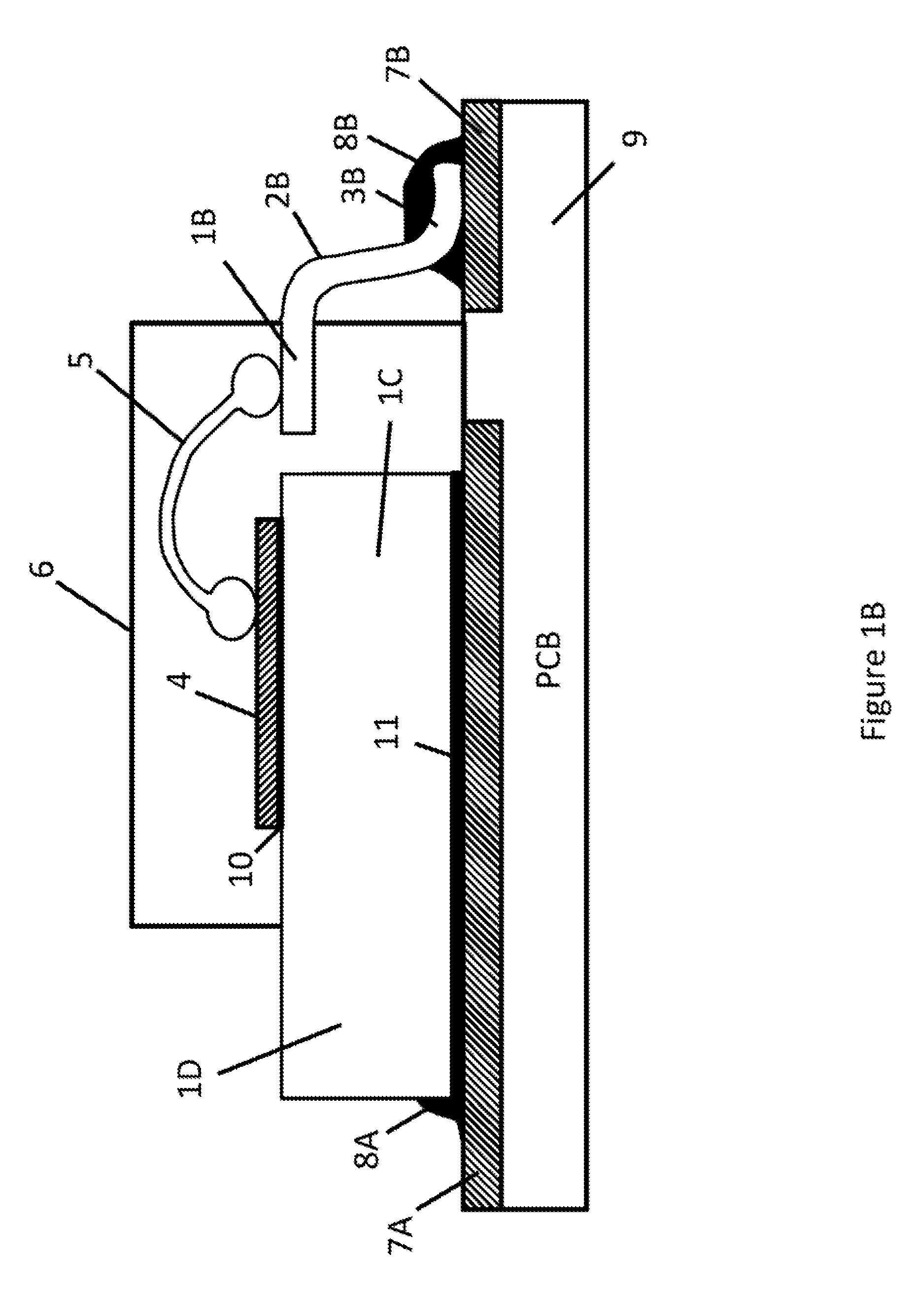
mechanical processes are imperfect and subject to unavoidable variability, leading to mismatches between the bottom of flat portion 3B and die pad 1C.
Aside from its poor coplanarity between the bottom of leads and the back of an exposed die pad and its inability to scale to thin package profiles, the need for manual placement of the solder under the heat tab is another disadvantage of conventional surface mount power packages.
This mechanical process, while faster than etching, creates several problems.
First, compressed metal exhibits mechanical stress not present in etched leadframes.
Stress can lead to cracking of plastic or silicon die contacting the stressed metal.
As a further complication, in leads mechanically thinned by stamping, the excess metal squeezes out the sides of the thinned lead and must be removed by trimming.
One major disadvantage of leaded package technology is that each package needs its own mold, commonly requiring an initial investment of over $100,000 USD.
The unintended consequence of high initial investment is that companies become more cautious about releasing new packages into the market, new package technology and capability become commercially available at a slower pace, and consequentially innovation and advancement slow to a snail's pace.
High initial investment and low UPH both adversely contribute to product cost.
Down time for changing the mold tool can be an hour or longer, reducing the average throughput and increasing production net cost per unit.
Guaranteeing coplanarity between exposed die pad 34D and the bottom of leads 33D in manufacturing however remains problematic.
As in the previous SO package description, maintaining good coplanarity between the bottom of exposed die pad 34O and leads 33O is problematic since the alignment is entirely mechanical and subject to unavoidable manufacturing variability.
In manufacturing however, maintaining coplanarity remains problematic especially in low-profile package designs.
Package area efficiency, the maximum die size divided by the external footprint, i.e. the lateral extent of the leads or plastic whichever is larger, is poor for leaded packages because a lot of space is wasted by the need to bend the lead down to the PCB surface.
Consequently, the die pad of a leadless package is naturally exposed on the package's underside, i.e. not isolated from the PCB, as an unavoidable artifact of its manufacturing process.
Because, however, the solder paste must be screened onto the PCB in advance, and an expensive temperature regulated reflow oven or belt furnace is required, manufacturing cost for reflow PCB manufacturing can be twice to four times the cost of simple wave-soldering, where the PCB and components are simply dipped in solder.
This higher PCB assembly cost represents one of the major disadvantages of leadless packaging.
While constituting a visibly identifiable feature, the exposed metal on the package vertical sidewall is not sufficient in area for soldering.
While the package dimensions may be standardized, there is no corresponding standardized size for the exposed die pad.
Such a package cannot be manufactured in the standard process described for QFN and DFN fabrications because sawing or punching unavoidably results in a perfectly vertical edge sidewall to the package with all the plastic and metal cut flush by the saw cutline.
For all of its advantages, one major disadvantage of the QFN / DFN leadless package is its inability to be used in wave-solder PCB factories.
Also, solder flow must be performed in expensive reflow ovens or belt furnaces making the entire PCB assembly process 2 to 4 times more expensive than that of simple wave-solder factory based production.
Moreover, visual inspection of leadless packages soldered to a PCB using simple automated camera inspection is impossible because the solder cannot be confirmed from the top view.
Instead expensive X-ray inspection equipment is required, adding cost and safety risk into reflow PCB manufacturing.
Nevertheless, despite its benefit in PCB manufacturing, the actual package manufacturing of leaded packages suffers from many issues including poor lead coplanarity, poor manufacturing control in the lead bending process, risk of plastic cracking during lead bending, risk of delamination between the plastic and leads, and inability to be scaled into low profile package, especially for package heights below 1 mm.
Poor coplanarity also renders leaded packages difficult to heat sink using exposed die pads because the package's bent leads do not consistently align with the bottom of the die pad or heat slug.
Because of long lead dimensions required to perform clamping during lead bending, the length of the conductive leads results in poor package and PCB areal efficiencies and results in excessive lead inductance, adversely affecting switching performance especially in power applications.
The mounting of power devices is especially problematic because special two-step soldering is required, first to solder the exposed die pad and heat tab to the PCB, and then to wave-solder the leads.
Variability in the lead-bending process combined with natural stochastic variations in the intervening solder thickness placed beneath the die pad result in unpredictable misalignments between the bottom of the bent leads and the PCB conductor, leading to poor connections, cold solder joints, intermittent contact, and degraded reliability.
Another disadvantage of leaded packages is their manufacturing inflexibility.
While equipment can generally be converted to accommodate different packages, the resulting factory downtime to convert a line from one package to another results in lost productivity and a lower UPH, thereby increasing per unit manufacturing costs.
Clearly from the above, no existing package meets the combined needs of the market.
Moreover, each class of surface-mount package used today requires completely different semiconductor package factories for manufacturing, forcing packaging companies to choose their markets with little chance to expand into new markets without incurring significant additional capital costs.

Method used


Image

  • Universal surface-mount semiconductor package
  • Universal surface-mount semiconductor package
  • Universal surface-mount semiconductor package

Examples


Embodiment Construction

[0258]The above-referenced application Ser. No. 14 / 056,287 and Provisional Applications Nos. 61 / 775,540 and 61 / 775,544 relate to inventive methods to make low profile wave-solder compatible semiconductor packages for integrated circuits. These patent applications disclose methods to manufacture low-profile footed packages in the same semiconductor IC packaging facilities presently used to fabricate gull wing leaded packages such as the SOP8 or SOT23. The patent applications also disclose methods to manufacture low-profile footed packages in facilities today used to manufacture leadless packages such as the QFN and DFN.

[0259]The above-referenced application Ser. No. 14 / 703,359 relates to inventive methods to make low profile wave-solder compatible power semiconductor packages for discrete power devices such as the DPAK and D2PAK and other custom leaded packages adapted for power integrated circuits using the same factories used today to manufacture thick, i.e. high profile, packages ...


PUM


Abstract

In the fabrication of semiconductor packages, a leadframe is formed by masking and etching a metal sheet from both sides, and a plastic block is formed over a plurality of dice attached to die pads in the leadframe. A laser beam is used to form individual plastic capsules for each package, and a second laser beam is used to singulate the packages by severing the metal conductors, tie bars and rails between the packages. A wide variety of different types of packages, from gull-wing footed packages to leadless packages, with either exposed or isolated die pads, may be fabricated merely by varying the patterns of the openings in the mask layers and the width of the plastic trenches created by the first laser beam.

Description

CROSS-REFERENCE TO RELATED APPLICATIONS[0001]This application is a continuation-in-part of application Ser. No. 14 / 056,287, filed Oct. 17, 2013, which claims the priority of Provisional Applications Nos. 61 / 775,540 and 61 / 775,544, both filed Mar. 9, 2013, and also a continuation-in-part of application Ser. No. 14 / 703,359, filed May 9, 2015. Each of the foregoing applications is incorporated herein by reference in its entirety.FIELD OF THE INVENTION[0002]This invention relates to semiconductor packaging including methods and apparatus designed to fabricate and use surface mount packages in printed circuit board assembly.BACKGROUND OF THE INVENTION[0003]Semiconductor devices and ICs are generally contained in semiconductor packages comprising a protective coating or encapsulant to prevent damage during handling and assembly of the components during shipping and when mounting the components on printed circuit boards. For cost reasons, the encapsulant is preferably made of plastic. In a...

Claims


Application Information

Patent Timeline
Patent Type & Authority Patents(United States)
IPC IPC(8): H01L21/44H01L23/31H01L21/48H01L21/50H01L21/78H01L21/268H01L21/3105H01L21/56H01L23/00H01L21/00H01L23/495
CPCH01L24/97H01L21/268H01L21/31058H01L21/4828H01L21/56H01L21/565H01L21/78H01L23/3107H01L23/4952H01L23/49551H01L23/49555H01L23/49562H01L23/49568H01L24/40H01L2224/45147H01L2224/4846H01L2224/48091H01L2224/48247H01L2224/48464H01L2224/49111H01L2224/49171H01L2224/73257H01L2224/73265H01L2224/92247H01L2224/97H01L2924/1305H01L2924/13055H01L2924/13091H01L2924/181H01L2924/00014H01L2924/00H01L2924/00012H01L2224/32245H01L23/49513H01L2224/0603H01L2224/16245H01L2224/40245H01L2924/00011H01L2224/37147H01L2224/84801H01L24/37H01L24/45H01L2224/45124H01L2224/45144H01L2224/8485H01L24/06H01L24/32H01L24/41H01L24/49H01L24/73H01L24/84H01L2224/4111H01L2224/73221H01L2924/01005H01L2924/01033H01L2224/85H01L2224/83H01L2224/05599H01L21/4825H01L21/4842H01L21/561H01L23/3114H01L23/49582H01L24/96
Inventor WILLIAMS, RICHARD K.LIN, KENG HUNG
Owner ADVENTIVE INT LTD
Why Eureka
Try Eureka