Lateral power device having low specific on-resistance and using high-dielectric constant socket structure and manufacturing method therefor
a technology of specific on-resistance and lateral power device, which is applied in the direction of semiconductor power device, electrical apparatus, basic electric elements, etc., can solve the problems of device specific on-resistance, low permittivity of siosub>2 /sub>, and confined specific on-resistance, etc., to achieve high breakdown voltage, uniform potential distribution, and high permittivity
- Summary
- Abstract
- Description
- Claims
- Application Information
AI Technical Summary
Benefits of technology
Problems solved by technology
Method used
Image
Examples
embodiment 1
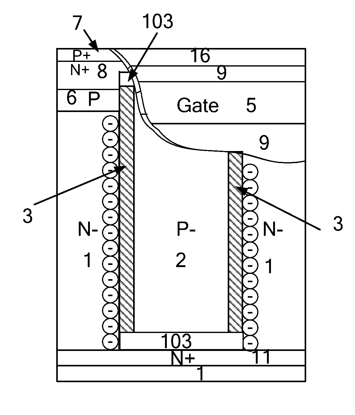
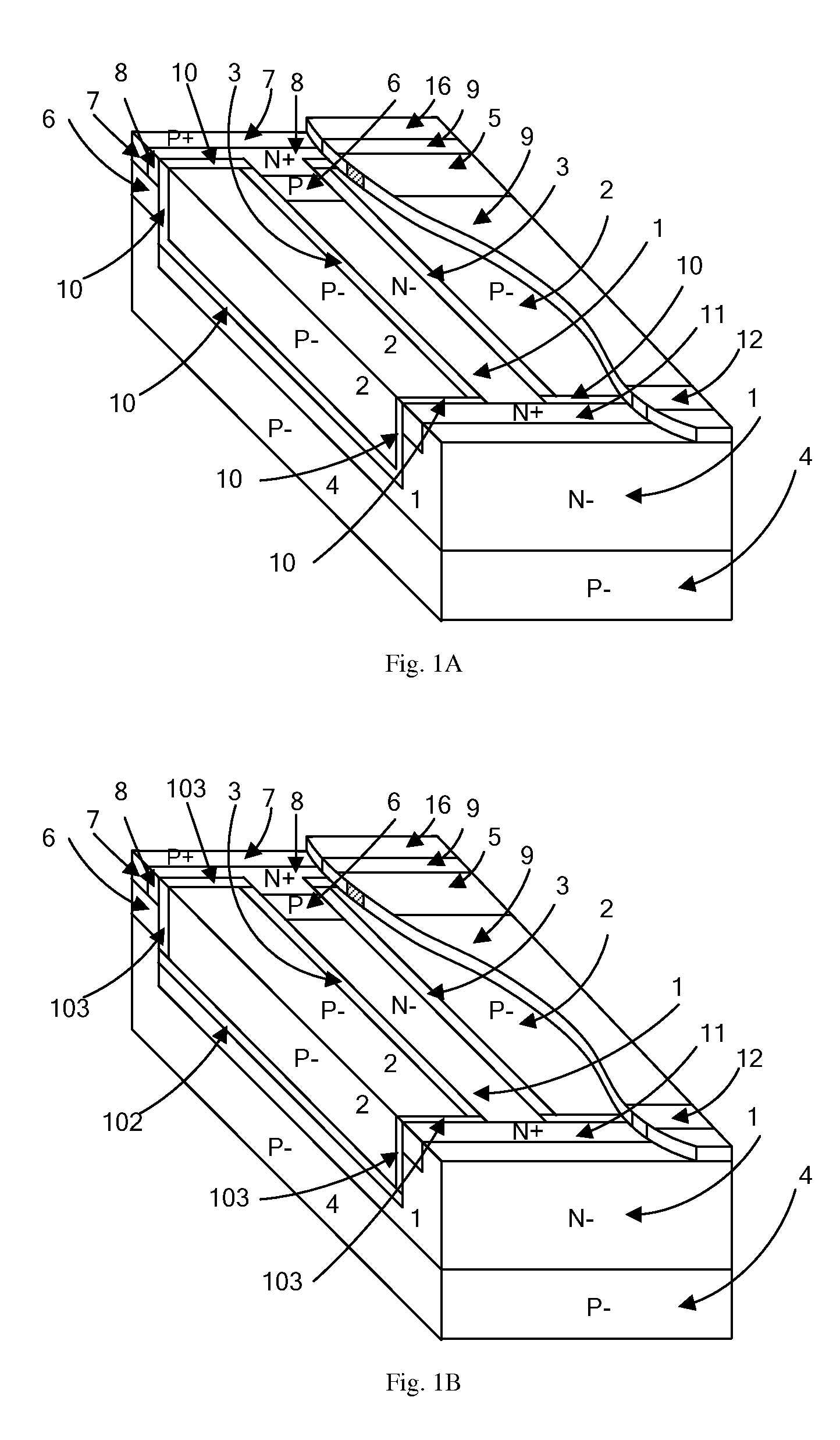
[0052]This embodiment uses the P− doped silicon as the material for substrate 4 and the first filler material 2 inside the isolation region, and uses the N doped conductive type silicon as the drift region 1. Besides, this embodiment 1 also comprises the channel region 6, ohm contact heavy doping region 7, source 8, gate 5, drain 11, drain contact 12, source contact 16, high permittivity material socket 3, the first dielectric layer 10 (including the bottom 102 and end face sidewall 103), and the second dielectric layer 9 using SiO2 or high permittivity material. At least two isolation regions are placed into the drift region 1; the drift region 1 and channel region 6 locate between the adjoining isolation regions; and each isolation extends from source 8 to drain 11; the boundary of isolation regions are formed by high permittivity material socket 3 and the first dielectric layer 10; the bottom 102 of the first dielectric layer 10 locates at the bottom of the first filler material ...
embodiment 2
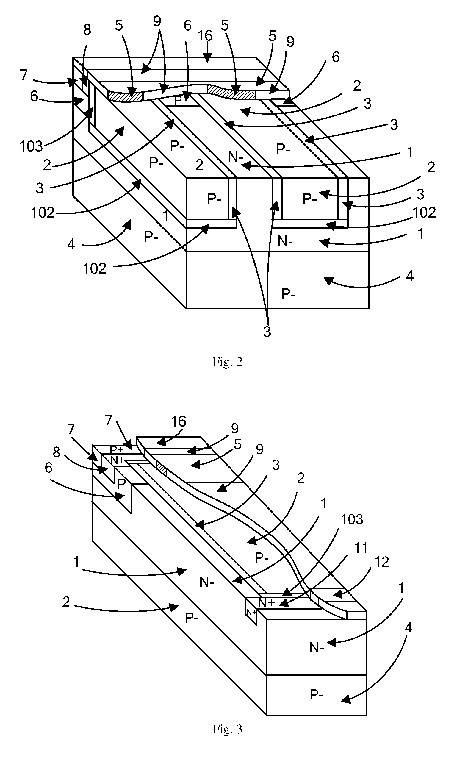
[0055]As shown in FIG. 5-7. This embodiment uses the P− silicon as the substrate 4, and uses the N− silicon as the drift region 1. The isolation regions are partially filled by the third filler material 51 at the side of the source. The third filler material uses the same material as the gate 5, and the gate 5 contacts the third filler material 51 through the via (the shadow part in the FIG. 5) on the second dielectric layer 9, the rest part of the isolations are filled by the first filler material 2, which is the same material as the high permittivity sockets 3. The source contact 16 connects the source 8 and ohm contact heavy doping region 7 through the via on the second dielectric layer 9, the drain 11 contacts drain contact through the via on the second dielectric layer 9.
[0056]Although this embodiment only uses the potential modulation effect of high permittivity to optimize the potential distribution without N&P alternating structure, whereas the high permittivity material tak...
embodiment 3
[0057]The difference between this embodiment and the embodiment 1 is that the material of first filler material 2 is N− silicon for this embodiment. Also, this embodiment uses the P− and N− as the silicon substrate 4 and drift region 1, respectively.
[0058]As the material of the first filler material 2 is not the P− silicon for this embodiment, the potential distribution optimization only relies on the modulation effect of the high permittivity material. However, the proportion of the high permittivity in the drift region is lower than that of the embodiment 2, the average permittivity improvement between drain 11 and source 8 is limited. Consequently, the breakdown voltage of this embodiment is lower than that of the embodiment 1. Although the N− silicon is used as the first filler material inside the isolation region, the N− silicon direct contacts the gate 5 but isolated from drain 11, the strong accumulation effect will happen in the entire drift region at the device on state lik...
PUM
 Abstract
Description
Claims
Application Information
 - R&D
- Intellectual Property
- Life Sciences
- Materials
- Tech Scout
- Unparalleled Data Quality
- Higher Quality Content
- 60% Fewer Hallucinations
Browse by: Latest US Patents, China's latest patents, Technical Efficacy Thesaurus, Application Domain, Technology Topic, Popular Technical Reports.
© 2025 PatSnap. All rights reserved.Legal|Privacy policy|Modern Slavery Act Transparency Statement|Sitemap|About US| Contact US: help@patsnap.com


