Organic light emitting diode display having thin film transistor substrate using oxide semiconductor

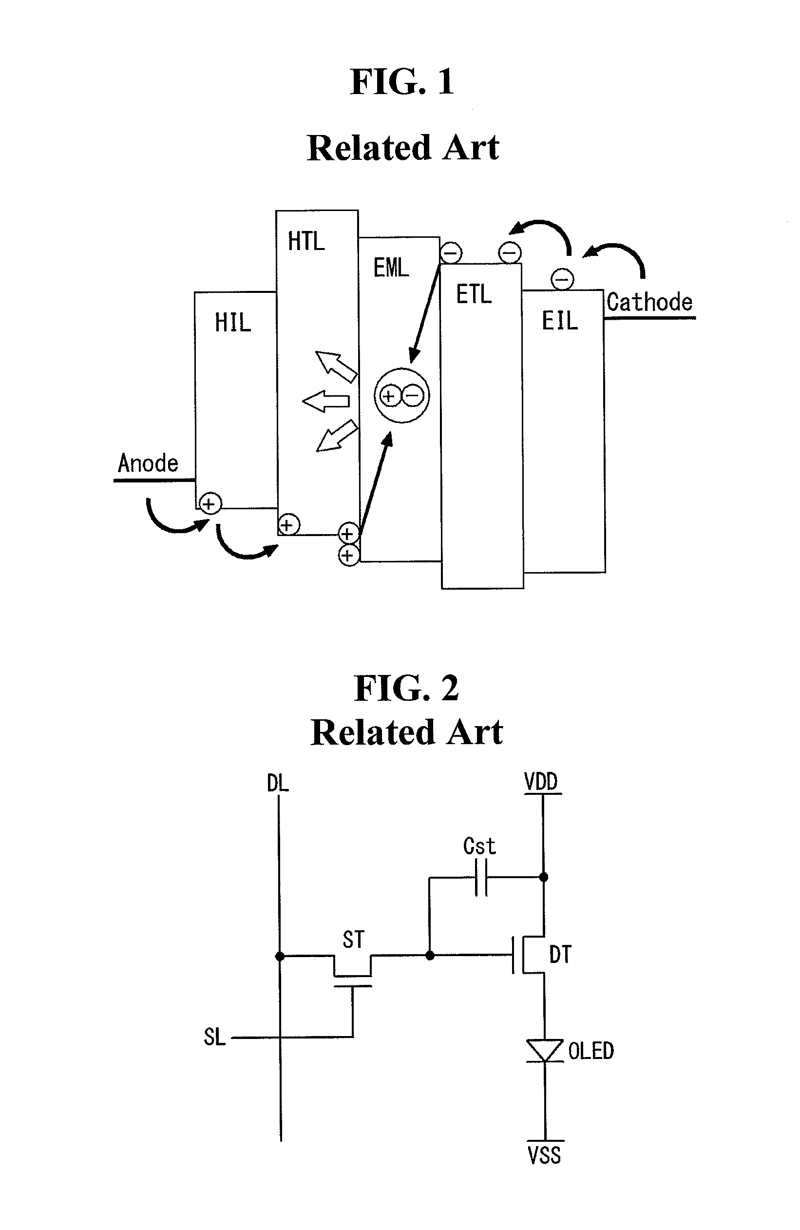
a technology of organic light-emitting diodes and thin film transistors, which is applied in the direction of semiconductor devices, diodes, electrical devices, etc., can solve the problems of many undesirable effects of thin film transistors, and achieve the effect of good current characteristics and reduced length

Active Publication Date: 2016-04-19
LG DISPLAY CO LTD
View PDF22 Cites 1 Cited by
  • Summary
  • Abstract
  • Description
  • Claims
  • Application Information

AI Technical Summary

Benefits of technology

[0032]The thin film transistor substrate having an oxide semiconductor layer according to present disclosure has the channel area and the source-drain area which are precisely defined by conductorizing the oxide semiconductor layer using the etch stopper as a mask. That is, the channel area can be formed as having the minimized length using the etch stopper. Further, the source-drain electrodes are connected to the conductorized source-drain areas of the oxide semiconductor layer, respectively. As the result, the channel area is not overlapped with the source-drain electrodes, and the thin film transistor having the good current characteristics can be acquired. In addition, when using the back exposure process, the gate electrode, the channel area and the etch stopper can be formed as having the same shape and area, so that even in the bottom gate structure, it is possible to get the merit of the top gate structure in which the parasitic capacitance of the gate-source electrodes and the gate-drain electrodes can be eliminated.

Problems solved by technology

This may cause many undesirable effects on the thin film transistor.

Method used


Image

  • Organic light emitting diode display having thin film transistor substrate using oxide semiconductor
  • Organic light emitting diode display having thin film transistor substrate using oxide semiconductor
  • Organic light emitting diode display having thin film transistor substrate using oxide semiconductor

Examples


first embodiment

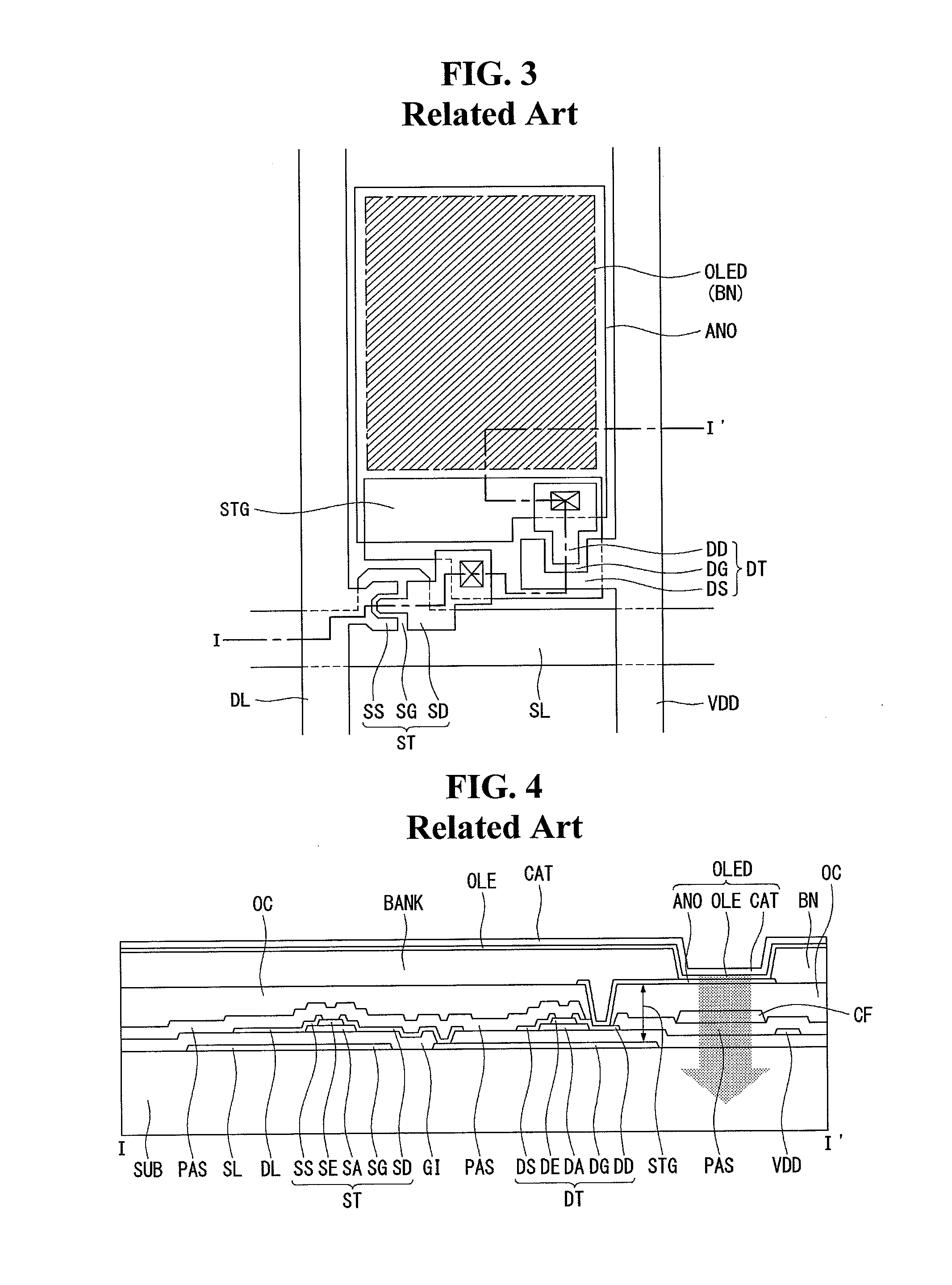
[0048]Referring to FIGS. 5 and 6, an organic light emitting diode display according to the present disclosure has gate electrodes SG and DG of the switching thin film transistor ST and the driving thin film transistor DT, respectively, formed on a substrate SUB. On the gate electrodes SG and DG, the gate insulator GI is deposited. The semiconductor layers SA and DA are formed on some portions of the gate insulator GI overlapping with the gate electrodes SG and DG. On the semiconductor layers SA and DA, the source electrodes SS and DS and the drain electrodes SD and DD are facing each other respectively with certain distance. The drain electrode SD of the switching thin film transistor ST is connected to the gate electrode DG of the driving thin film transistor DT via the contact hole penetrating the gate insulator GI. The passivation layer PAS is deposited on the substrate SUB having the switching thin film transistor ST and the driving thin film transistor DT.

[0049]Especially, when...

second embodiment

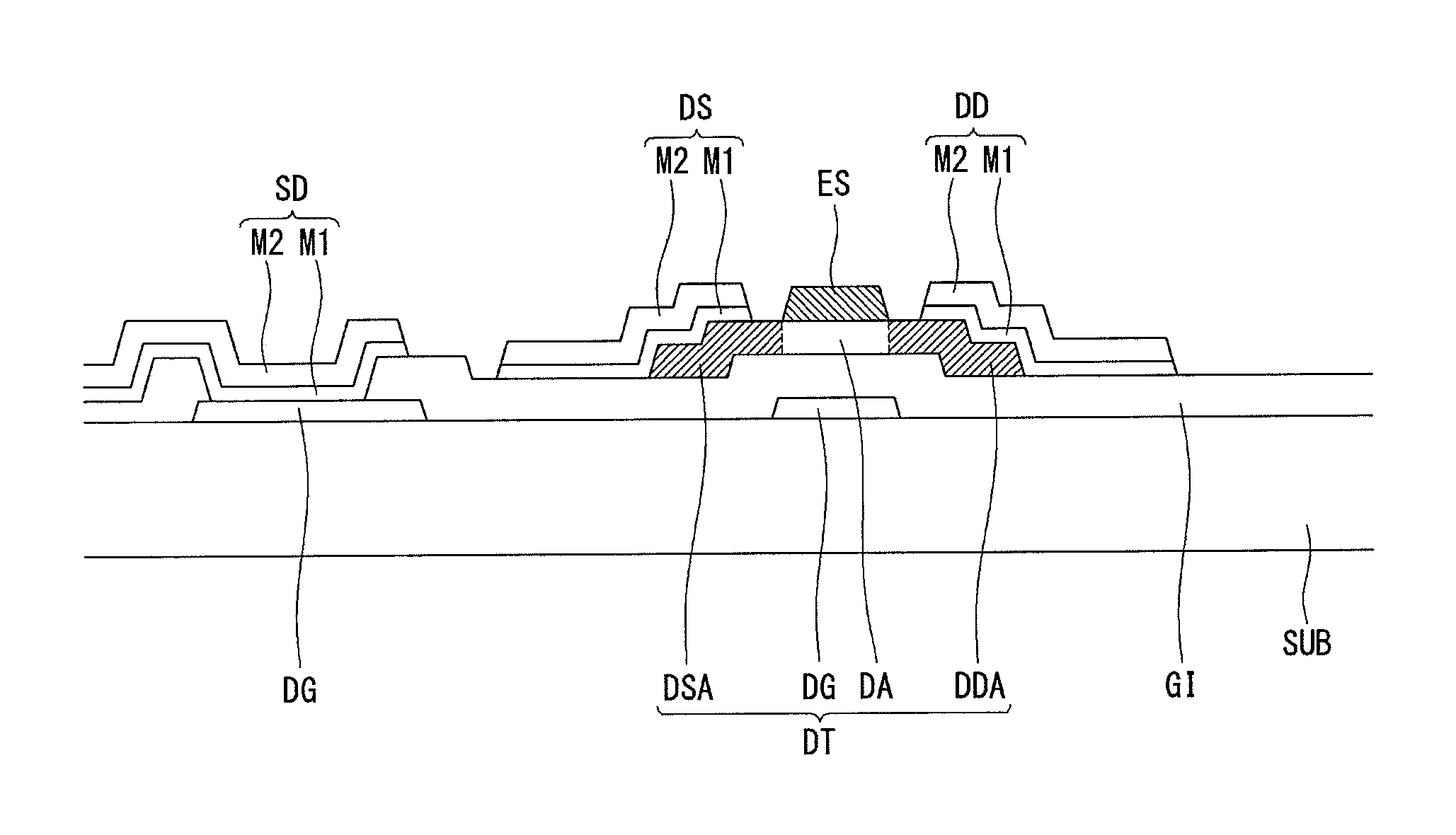
[0077]In the second embodiment, the channel areas SA and DA and the etch stopper ES is defined and / or formed using the shape of the gate electrodes SG and DG. That is, the channel area of the thin film transistor is defined by the pattern of the gate electrode. In detail, the gate electrode is formed by the designed channel area in the thin film transistor, the etch stopper is formed by the back exposure method using the gate electrode as a mask, and the channel area and the source-drain areas are defined using the etch stopper.

[0078]Referring to FIGS. 9 and 10, the organic light emitting diode display according the second embodiment includes a gate electrode SG of the switching thin film transistor ST and a gate electrode DG of the driving thin film transistor DT formed on a substrate SUB. On the gate electrodes SG and DG, a gate insulating layer GI is deposited. On the gate insulating layer GI, a semiconductor layer SEM is formed in which the semiconductor layer SEM includes the c...


PUM


Abstract

Provided is a thin film transistor having an oxide semiconductor material for an organic light emitting diode display and a method for manufacturing the same. The organic light emitting diode display includes a gate electrode formed on a substrate; a gate insulating layer formed on the gate electrode; a semiconductor layer formed on the gate insulating layer to overlap with the gate electrode, and including a channel area and source and drain areas which extend from the channel area to both outsides, respectively and are conductorized; an etch stopper formed on the channel area and exposing the source area and the drain area; a source electrode contacting portions of the exposed source electrode; and a drain electrode contacting portions of the exposed drain electrode.

Description

CROSS-REFERENCE TO RELATED APPLICATION[0001]This application claims the benefit of and priority to Korea Patent Application No. 10-2013-0090499 filed on Jul. 30, 2013, which is hereby incorporated by reference for all purposes as if fully set forth herein.BACKGROUND OF THE INVENTION[0002]1. Field of the Invention[0003]The present disclosure relates to a thin film transistor substrate having an oxide semiconductor material for an organic light emitting diode display and a method for manufacturing the same. Especially, the present disclosure relates to an organic light emitting diode display having a thin film transistor substrate in which a channel area and a source-drain area in an oxide semiconductor layer are defined by an etch stopper layer and a method for manufacturing the same.[0004]2. Discussion of the Related Art[0005]Nowadays, various flat panel display devices are developed for overcoming many drawbacks of the cathode ray tube such as heavy weight and bulk volume. The flat...

Claims


Application Information

Patent Timeline
Patent Type & Authority Patents(United States)
IPC IPC(8): H01L27/32H01L29/66H01L29/78H01L29/786H01L29/417H01L27/12
CPCH01L29/7869H01L27/1225H01L27/3272H01L29/41733H01L29/66969H01L27/3262H01L29/7818H10K59/126H01L29/78618H10K59/1213H10K59/1201H01L21/44H01L21/47635H01L29/42356
Inventor HONG, SUNGJINAHN, BYUNGCHULKOH, YOUNGJUNAM, WOOJINTANI, RYOSUKE
Owner LG DISPLAY CO LTD
Why Eureka
Try Eureka