
Overlay performance for a fin field effect transistor device

a transistor and field effect technology, applied in semiconductor devices, semiconductor/solid-state device details, electrical apparatus, etc., can solve the problems of poor image quality, overlay mark optimized for traditional process might not be suitable in the overlay mark optimized for traditional process might not be suitable for some fin-based alignment mask concepts, etc., to achieve the effect of improving overlay performance and avoiding finification

Inactive Publication Date: 2015-12-22
ALSEPHINA INNOVATIONS INC
View PDF6 Cites 4 Cited by
  • Summary
  • Abstract
  • Description
  • Claims
  • Application Information

AI Technical Summary

Benefits of technology

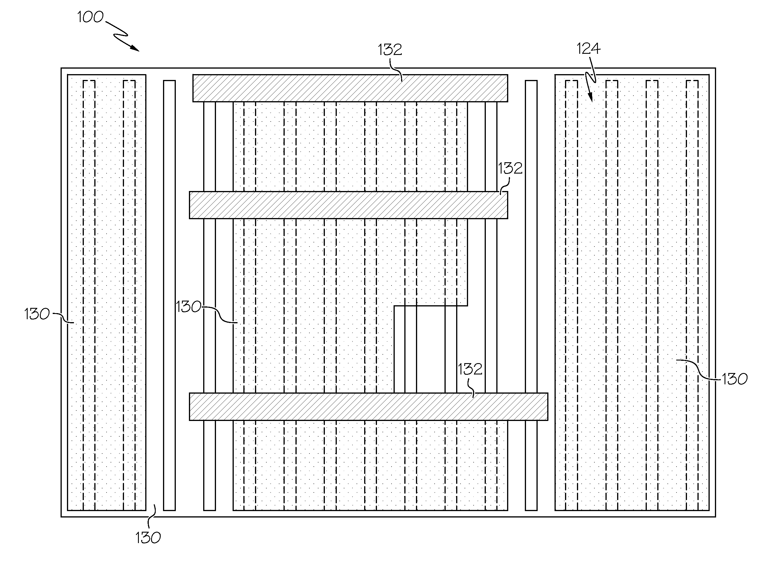
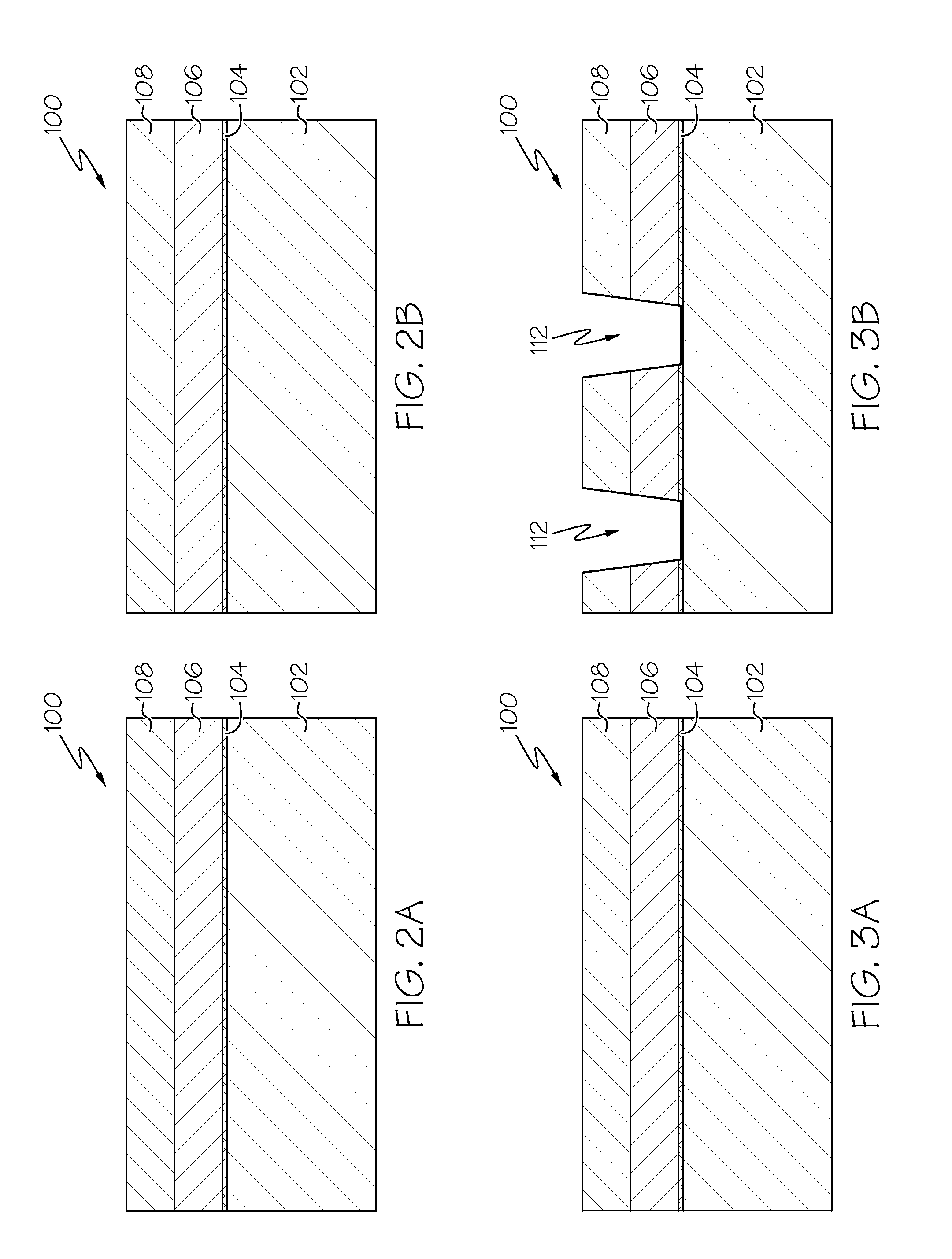
[0006]In general, approaches for improving overlay performance for an integrated circuit (IC) device (e.g., fin field effect transistors (FinFETs)) are provided. Specifically, the IC device is provided with an oxide layer and a pad layer formed over a substrate, wherein the oxide layer comprises an alignment / overlay mark, a fin cut (FC) mask formed over the pad layer, an oxide deposited in a set of openings formed through the pad layer and into the substrate, and a mandrel layer deposited over the oxide material and the pad layer. The IC device further comprises a set of fins patterned therein, following deposition of the mandrel layer. With this approach, the alignment and overlay mark is provided with the fin cut (FC) layer and, therefore, avoids finification.

Problems solved by technology

Over time, these overlay performance requirements have become more stringent as design rules shrink.
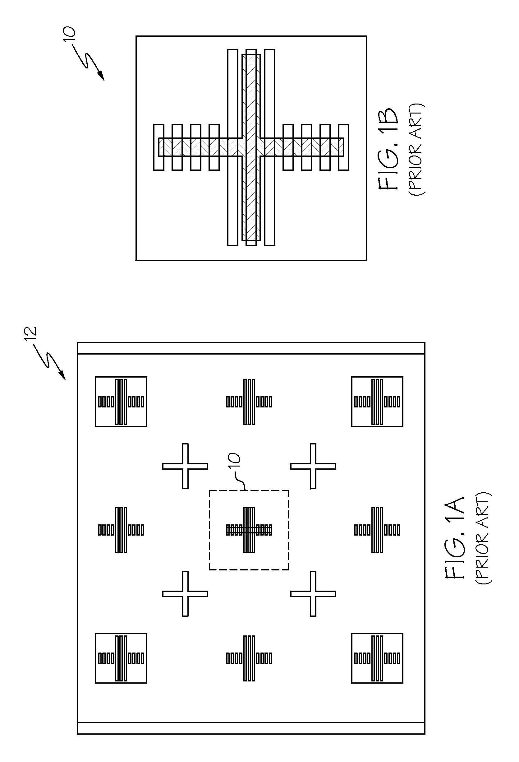
An overlay mark optimized for traditional process might not be suitable in some fin-based alignment mask concepts due to changes in lithography and etching process conditions.
In this case, image quality is poor for mark 10 because the fin profile, line end shortness, and line edge roughness for the fin greatly impact overlay measurement quality.

Method used


Image

  • Overlay performance for a fin field effect transistor device
  • Overlay performance for a fin field effect transistor device
  • Overlay performance for a fin field effect transistor device

Examples


Embodiment Construction

[0035]Exemplary embodiments will now be described more fully herein with reference to the accompanying drawings, in which exemplary embodiments are shown. Described are approaches for improving overlay performance for an integrated circuit (IC) device. Specifically, the IC device (e.g., a FinFET device) is provided with an oxide layer and a pad layer formed over a substrate, wherein the oxide layer includes an alignment and overlay mark, a fin cut (FC) mask formed over the pad layer, an oxide deposited in a set of openings formed through the pad layer and into the substrate, and a mandrel layer deposited over the oxide material and the pad layer. The IC device further comprises a set of fins patterned therein, following deposition of the mandrel layer. With this approach, the alignment and overlay mark is provided with the FC layer to avoid finification.

[0036]It will be appreciated that this disclosure may be embodied in many different forms and should not be construed as limited to...


PUM


Abstract

Approaches for improving overlay performance for an integrated circuit (IC) device are provided. Specifically, the IC device (e.g., a fin field effect transistor (FinFET)) is provided with an oxide layer and a pad layer formed over a substrate, wherein the oxide layer comprises an alignment and overlay mark, an oxide deposited in a set of openings formed through the pad layer and into the substrate, a mandrel layer deposited over the oxide material and the pad layer, and a set of fins patterned in the IC device without etching the alignment and overlay mark. With this approach, the alignment and overlay mark is provided with the fin cut (FC) layer and, therefore, avoids finification.

Description

BACKGROUND[0001]1. Technical Field[0002]This invention relates generally to the field of semiconductors, and more particularly, to improving alignment / overlay performance for a fin field effect transistor device.[0003]2. Related Art[0004]A typical integrated circuit (IC) chip includes a stack of several levels or sequentially formed layers of shapes. Each layer is stacked or overlaid on a prior layer and patterned to form the shapes that define devices (e.g., fin field effect transistors (FinFETs)) and connect the devices into circuits. In a typical state of the art complementary insulated gate FinFET process, such as what is normally referred to as CMOS, layers are formed on a wafer to form the devices on a surface of the wafer. Further, the surface may be the surface of a silicon layer on a silicon on insulator (SOI) wafer. A simple FinFET includes a gate layer rectangle on a silicon island formed from the silicon surface layer. Each of these layers of shapes, also known as mask l...

Claims


Application Information

Patent Timeline
Patent Type & Authority Patents(United States)
IPC IPC(8): H01L21/336H01L21/762H01L21/308
CPCH01L21/3081H01L21/76224H01L23/544H01L2223/5442H01L2223/54426H01L2223/54453H01L2924/0002H01L21/845H01L2924/00
Inventor HU, ZHENYUWEI, ANDYZHANG, QICARTER, RICHARD J.SHEN, HONGLIANGPHAM, DANIELMURALIDHARAN, SRUTHI
Owner ALSEPHINA INNOVATIONS INC
Learn More