
Method for fabrication of ceramic dielectric films on copper foils

Inactive Publication Date: 2015-03-10
UCHICAGO ARGONNE LLC
View PDF8 Cites 0 Cited by
  • Summary
  • Abstract
  • Description
  • Claims
  • Application Information

AI Technical Summary

Benefits of technology

The present invention is about a method to make a special ceramic material called PLZT on a copper surface. This material can be used to make thin films that can be embedded in printed circuit boards. The method is simple and doesn't require any extra layers or gases to control its properties. The technique uses a simple inert gas atmosphere and does not require any special gas mixtures or foreign substances. The resulting thin film has a high capacitance density, making it useful for several applications.

Problems solved by technology

Base metal foils are subject to undesirable oxidation and require low oxygen partial pressures during high temperature annealing for formation of the desired crystalline phase of the ceramic that exhibits high-K.
The low oxygen partial pressures, however, can result in complications such as high dielectric losses due to reduction of dielectric materials, suppression of dielectric constant due to reactions between the thin film dielectrics and the substrates of metal foils.
The in-air processing capability cannot be extended to perovskites deposited onto copper substrates, because the ease with which copper forms a copper oxide (Cu2O) layer under such processing conditions.

Method used


Image

  • Method for fabrication of ceramic dielectric films on copper foils
  • Method for fabrication of ceramic dielectric films on copper foils
  • Method for fabrication of ceramic dielectric films on copper foils

Examples


examples

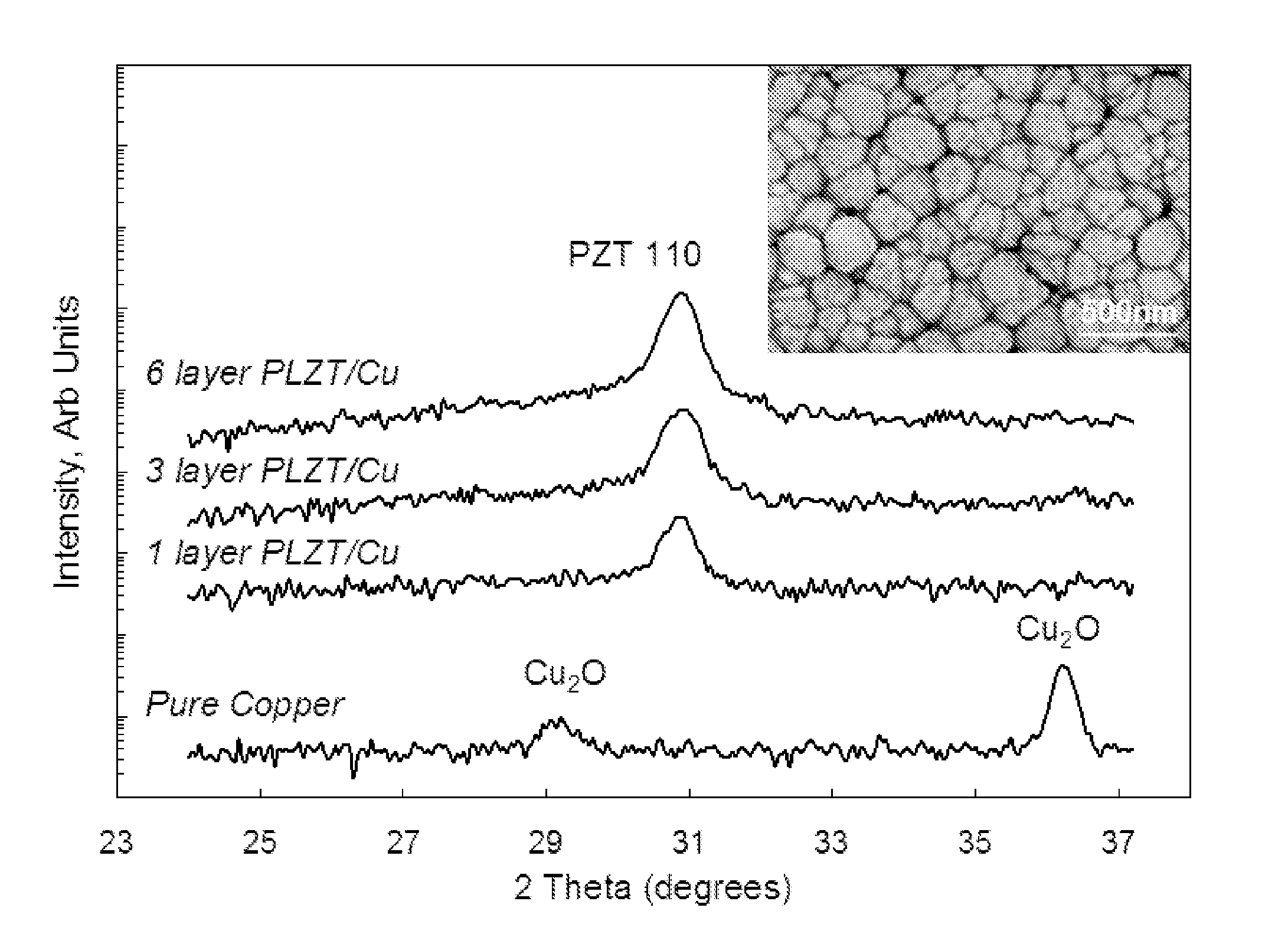
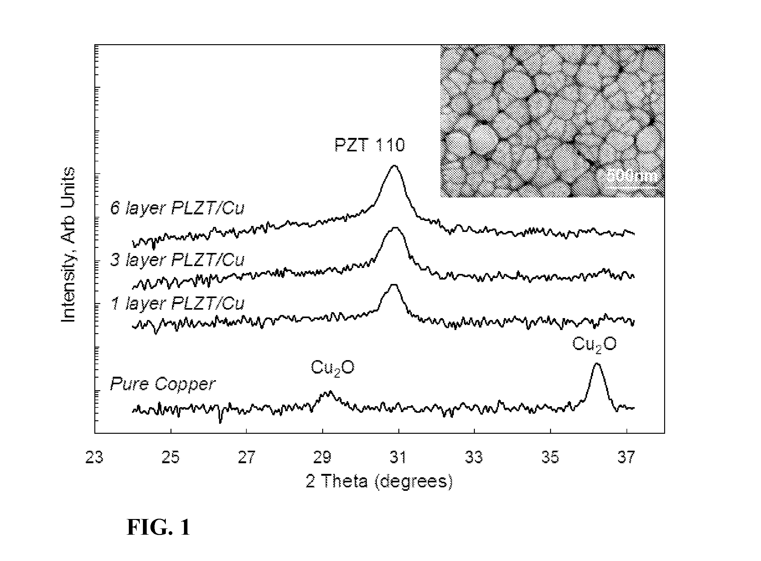
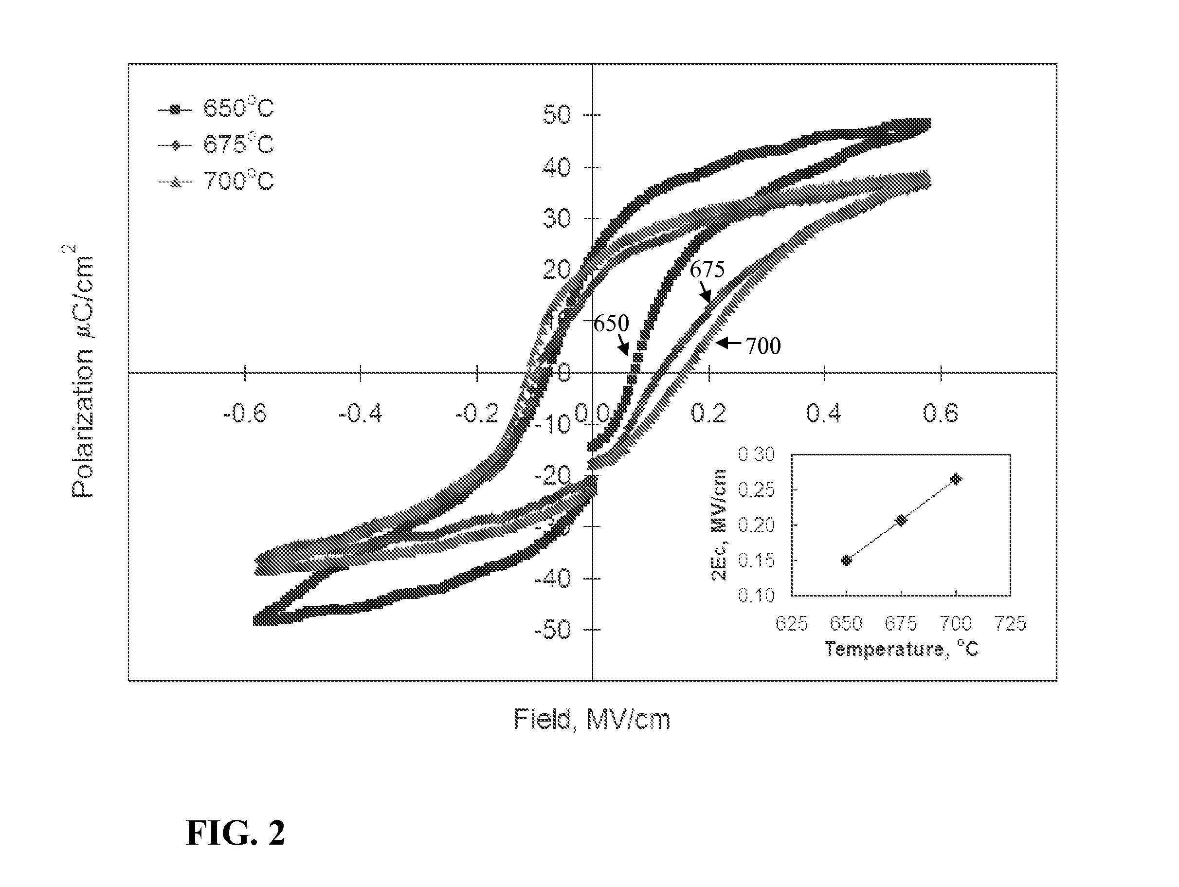
[0021]Thin films of Pb0.92La0.08Zr0.52Ti0.48O3 (PLZT 8 / 52 / 48) were prepared by sol-gel synthesis using lead acetate trihydrate, titanium isopropoxide, zirconium propoxide, lanthanum nitrate hexahydrate, and 2-MOE. A 20 mol % excess of lead was used in the starting solution to compensate for the lead loss during the high temperature crystallization. A detailed procedure for the solution synthesis is reported elsewhere [9]. Copper substrates (0.5 mm thick; 99.8% pure, ESPI Metals) were polished with a 1 μm diamond paste to a RMS surface roughness of about 5 nm, and then ultrasonically cleaned in acetone and methanol prior to coating. The 0.5M PLZT stock solution was spin coated onto the substrate at about 3000 revolutions-per-minute (rpm) for about 30 seconds (sec) and dried in a furnace at about 250° C. in air for about 10 minutes (min). The film was then pyrolyzed at about 450° C. for about 18 min under flowing N2 (99.999%, 500 standard cubic centimeters per minute, sccm) using a he...


PUM

PropertyMeasurementUnit
Temperatureaaaaaaaaaa

Abstract

The present invention provides a method for fabricating a ceramic film on a copper foil. The method comprises applying a layer of a sol-gel composition onto a copper foil. The sol-gel composition comprises a precursor of a ceramic material suspended in 2-methoxyethanol. The layer of sol-gel is then dried at a temperature up to about 250° C. The dried layer is then pyrolyzed at a temperature in the range of about 300 to about 450° C. to form a ceramic film from the ceramic precursor. The ceramic film is then crystallized at a temperature in the range of about 600 to about 750° C. The drying, pyrolyzing and crystallizing are performed under a flowing stream of an inert gas. In some embodiments an additional layer of the sol-gel composition is applied onto the ceramic film and the drying, pyrolyzing and crystallizing steps are repeated for the additional layer to build up a thicker ceramic layer on the copper foil. The process can be repeated one or more times if desired.

Description

CROSS-REFERENCE TO RELATED APPLICATIONS[0001]This application claims the benefit of U.S. Provisional Application Ser. No. 61 / 183,148, filed on Jun. 2, 2009, which is incorporated herein by reference in its entirety.CONTRACTUAL ORIGIN OF THE INVENTION[0002]The United States Government has rights in this invention pursuant to Contract No. W-31-109-ENG-38 between the United States Government and The University of Chicago and / or pursuant to Contract No. DE-AC02-06CH11357 between the United States Government and UChicago Argonne, LLC representing Argonne National Laboratory.FIELD OF THE INVENTION[0003]This invention relates to preparation of ceramic dielectric films. More particularly, the invention relates to methods for preparation of ceramic dielectric films on copper foils.BACKGROUND OF THE INVENTION[0004]The development of power electronic devices with improved performance, increased reliability, compact size, and reduced weight requires the passive components to be embedded within ...

Claims


Application Information

Patent Timeline
IPC IPC(8): B05D7/00C04B35/491C04B35/624C23C18/12C23C26/00H01G4/12
CPCC23C26/00C04B35/491C04B35/624C23C18/1208C23C18/1225C23C18/1241C23C18/1254C23C18/1283H01G4/1218H01G4/1245C04B2235/3227C04B2235/3232C04B2235/3244C04B2235/3296C04B2235/441C04B2235/443C04B2235/449C04B2235/6562C04B2235/6565C04B2235/6584C04B2235/768Y10T428/24355Y10T428/266C23C18/1204C23C18/1295H01G13/04
Inventor MA, BEIHAINARAYANAN, MANOJDORRIS, STEPHEN E.BALACHANDRAN, UTHAMALINGAM
Owner UCHICAGO ARGONNE LLC
Learn More