Vertical SOI bipolar junction transistor and manufacturing method thereof

a technology of bipolar junction transistor and soi, which is applied in the field of microelectronics and solid-state electronics, can solve the problems of affecting the dc characteristics of the transistor, the inability to easily scale down the lateral soi bjt device, and the limited performance of such devices, and achieves good compatibility and high integration density

Inactive Publication Date: 2014-01-14
SHANGHAI INST OF MICROSYSTEM & INFORMATION TECH CHINESE ACAD OF SCI
View PDF3 Cites 2 Cited by
  • Summary
  • Abstract
  • Description
  • Claims
  • Application Information

AI Technical Summary

Benefits of technology

[0006]The present invention provides a vertical SOI bipolar junction transistor with high integration density and good compatibility and a manufacturing method thereof.

Problems solved by technology

Even though lateral SOI BJT devices are easier to be integrated with SOI CMOS, the performance of such devices is limited.
However, the base width has a direct effect on transistor gain, thereby influencing the DC characteristics of the transistor.
In a word, the base width has great influence on the transistor characteristics, and the lateral SOI BJT devices cannot be easily scaled down.
In the conventional vertical SOI BJT, the bulk silicon BJT technology is applied to SOI substrate, thereby such a BJT is unsuitable for the integration with high-performance SOI CMOS.
There are two problems: On the one hand, the shallow trench isolation technology is very complicated and thereby increases the integration cost; On the other hand, the extraction electrode with ohmic contact formed by high dose rate ion implantation raises the area, and thereby lower the density of integration.
Such a high bias is not compatible with conventional SOI CMOS techniques, thus the buried oxide layer of the SOI BJT active region has to be thinned and a graphical SOI substrate is required.
However, there are two problems adopting the graphical SOI substrate: (1) it is hard to be aligned in photolithography; (2) it makes the SOI BJT manufacturing process more complicated.

Method used


Image

  • Vertical SOI bipolar junction transistor and manufacturing method thereof
  • Vertical SOI bipolar junction transistor and manufacturing method thereof
  • Vertical SOI bipolar junction transistor and manufacturing method thereof

Examples


first embodiment

[0039

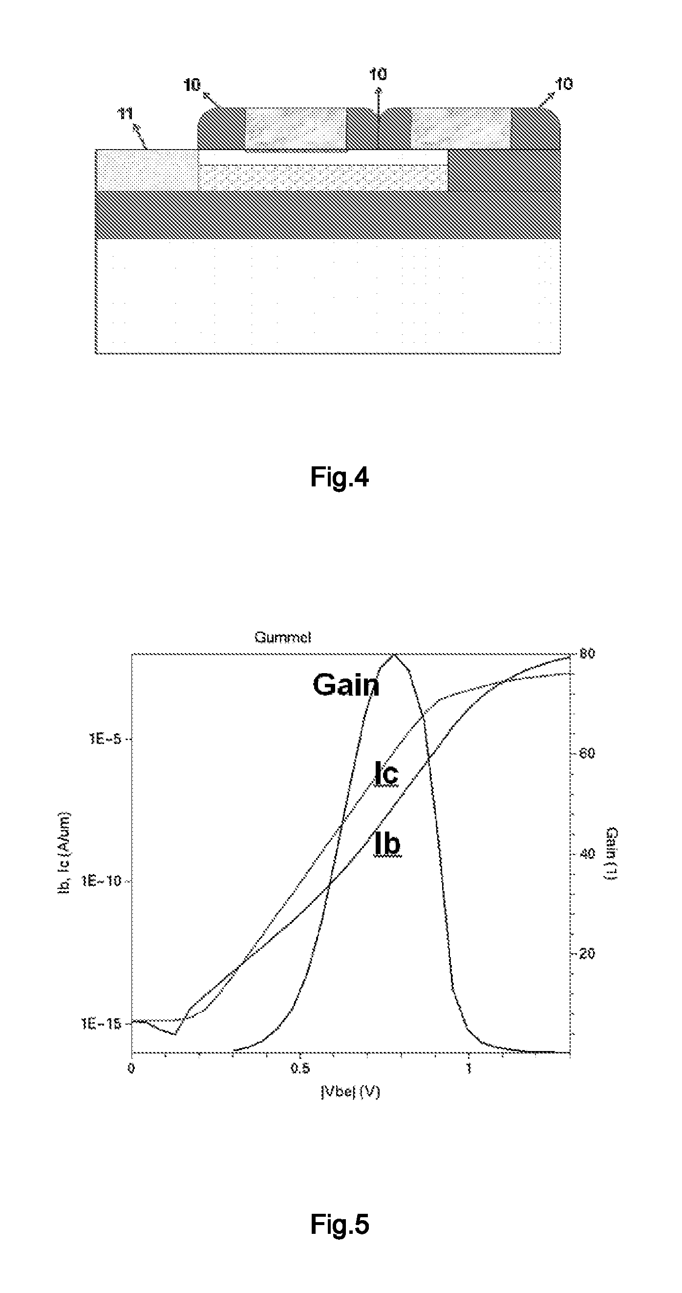
[0040]The present invention relates to a vertical silicon-on-insulator (SOI) bipolar junction transistor (BJT) and a method for manufacturing thereof. Such a vertical SOI BJT realizes a simple double poly silicon technology on SOI. One poly silicon structure means n+ poly silicon emitter which is used for reducing surface recombination velocity of the emitter, so as to improve the emitter injection efficiency and increase the current gain; on the other hand, the impurities in n+ poly silicon emitter can diffuse and form shallow emitter junction. Another poly silicon structure means p+ poly silicon base electrode as a outlet of the base region which can reduce the effective area of the device. According the present invention, the isolation between emitter and base electrode and the isolation between emitter and collector electrode utilize side-wall spacer process in MOS integrated circuit instead normal shallow trench isolation process, which can realize self-alignment, reduce t...

second embodiment

[0052

[0053]The present embodiment provides a NPN type double poly silicon vertical SOI bipolar junction transistor with side-wall spacer and the method for manufacturing thereof.

[0054]The manufacturing method is as follow:

[0055]First, form a SOI BJT active region on an SOI substrate by STI process of integrated circuit.

[0056]Next, a collector region and a base region located in the active region are formed by ion implantation. Wherein, the collector region is formed by doping N-type impurity into the active region with ion implantation process, the doping deep close to the SOI BOX. The base region is formed by implanting P-type impurity into the active region deep close to the surface. The forming of the collector region and the base region adopts a retrograde doping process which has a deep implantation before a shallow implantation. The retrograde doping process can obtain a thinner base region, so as to increase the current gain of transistor, on the other hand, the doping dose o...


PUM


Abstract

The present invention discloses a vertical SOI bipolar junction transistor and a manufacturing method thereof. The bipolar junction transistor includes an SOI substrate from down to up including a body region, a buried oxide layer and a top silicon film; an active region located in the top silicon film formed by STI process; a collector region located in the active region deep close to the buried oxide layer formed by ion implantation; a base region located in the active region deep close to the top silicon film formed by ion implantation; an emitter and a base electrode both located over the base region; a side-wall spacer located around the emitter and the base electrode. The present invention utilizing a simple double poly silicon technology not only can improve the performance of the transistor, but also can reduce the area of the active region in order to increase the integration density. Furthermore, the present invention utilizes side-wall spacer process to improve the compatibility of SOI BJT and SOI CMOS, which simplifies the SOI BiCMOS process and thus reduce the cost.

Description

CROSS REFERENCE TO RELATED PATENT APPLICATION[0001]The present application is the US national stage of PCT / CN2010 / 075156 filed on Jul. 14, 2010, which claims the priority of the Chinese patent application No. 200910201332.5filed on Dec. 17, 2009, which application is incorporated herein by reference.FIELD OF THE INVENTION[0002]The present invention relates to the microelectronics and solid state electronics fields and more particularly to a vertical silicon-on-insulator (SOI) bipolar junction transistor (BJT) and a manufacturing method thereof.BACKGROUND OF THE INVENTION[0003]Owing to the rapid development of the mobile communication industry, the demand for radio frequency integrated circuits (RFIC) has increased tremendously and the RFIC technology filed is getting very competitive. BiCMOS, refers to the integration of bipolar junction transistors and CMOS technology into a single integrated circuit device, is widely used and has been quiet successful in the RFIC technology filed ...

Claims


Application Information

Patent Timeline
Patent Type & Authority Patents(United States)
IPC IPC(8): H01L21/331
CPCH01L29/7317H01L29/66265
Inventor CHEN, JINGLUO, JIEXINWU, QINGQINGZHOU, JIANHUAHUANG, XIAOLUWANG, XI
Owner SHANGHAI INST OF MICROSYSTEM & INFORMATION TECH CHINESE ACAD OF SCI
Why Eureka
Try Eureka