Method of manufacturing vertically aligned nanotubes, method of manufacturing sensor structure, and sensor element manufactured thereby
a manufacturing method and nanotube technology, applied in the field of manufacturing well-aligned nanotubes and a manufacturing method of sensor elements, can solve the problems of difficult formation of well-aligned free-standing nanotubes and easy damage of nanotubes, and achieve the effects of simple method, excellent performance and low cos
- Summary
- Abstract
- Description
- Claims
- Application Information
AI Technical Summary
Benefits of technology
Problems solved by technology
Method used
Image
Examples
first embodiment
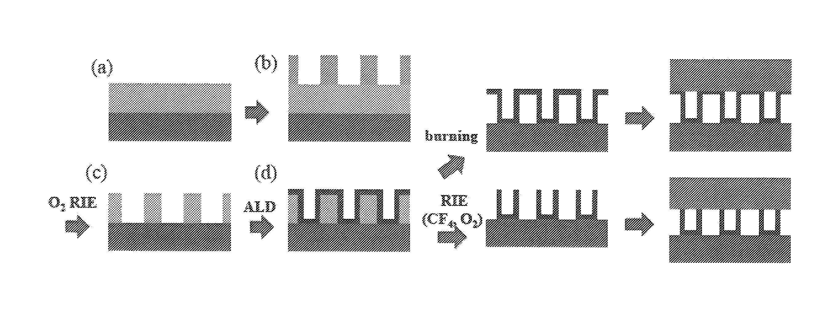
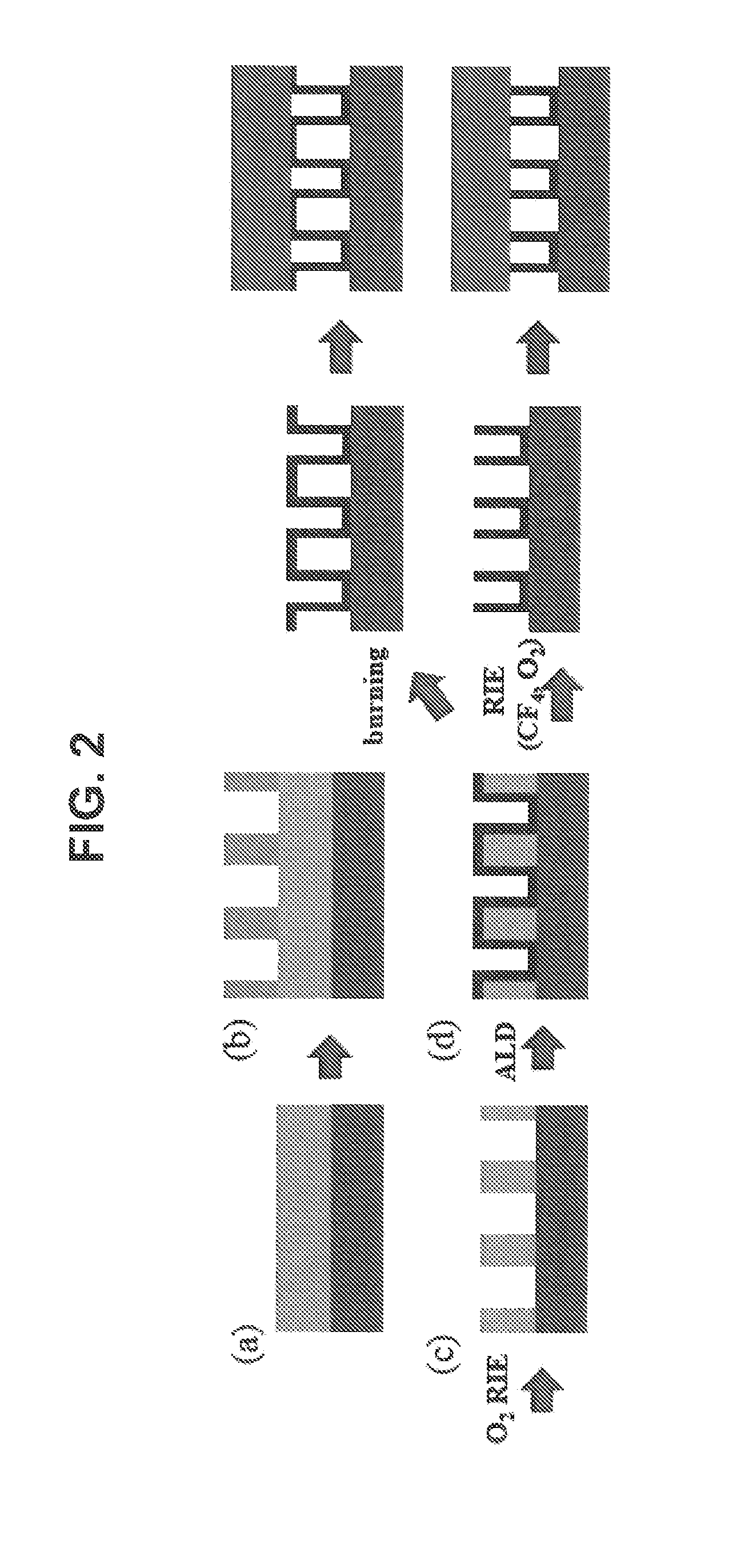
[0053]A method of manufacturing nanotubes using an organic template according to a first embodiment of the invention mainly includes four processes: 1) a process of forming a polymer film and an AAO (anodic aluminum oxide) mask; 2) a process of forming an organic template through a plasma etching method; 3) a process of forming nanotubes through an ALD method; and 4) a process of removing the organic template.
[0054]The polymer film can be formed by using various well-known organic materials through well-known film forming methods. In the embodiment, a polyimide film (hereinafter, referred to as a “PI film”) that is formed by spin-coating an amic acid and, after that, performing thermal treatment is used. More specifically, according to the method of forming the PI film, an 11 wt % amic acid dissolved in an NMP solution is spin-coated on an ITO glass substrate at 3,000 rpm, so that a film having a thickness of about 1,000 nm is formed. Next, the resulting film is thermally treated fo...
second embodiment
[0061]In a second embodiment of the invention, a gas sensor having TiO2 nanotubes is manufactured. The processes of manufacturing the organic template and forming the Au thin film are the same as those in the first embodiment. The TiO2 nanotubes are formed as follows.
[0062]In order to form the nanotubes, an TiO2 thin film is formed on the PI template, which is formed to be the same as that of the first embodiment, by using an ALD method. As a precursor for the TiO2 ALD process, TTIP and H2O are used. The precursor is injected for 0.5 seconds, exposed for 3 seconds, and purged for 3 seconds. These processes are alternately performed, so that a TiO2 layer having a thickness of 10 nm is formed. At this time, the deposition temperature is set to 250° C. As a result, an anatase phase is formed.
[0063]Although the ZnO and the TiO2 are described in the embodiments of the invention, various materials such as HfO2 and WO3 available for the ALD process can be adapted. In addition, various synt...
PUM
| Property | Measurement | Unit |
|---|---|---|
| thickness | aaaaa | aaaaa |
| size | aaaaa | aaaaa |
| size | aaaaa | aaaaa |
Abstract
Description
Claims
Application Information
 - R&D
- Intellectual Property
- Life Sciences
- Materials
- Tech Scout
- Unparalleled Data Quality
- Higher Quality Content
- 60% Fewer Hallucinations
Browse by: Latest US Patents, China's latest patents, Technical Efficacy Thesaurus, Application Domain, Technology Topic, Popular Technical Reports.
© 2025 PatSnap. All rights reserved.Legal|Privacy policy|Modern Slavery Act Transparency Statement|Sitemap|About US| Contact US: help@patsnap.com


