Active matrix type display apparatus and driving method thereof
a display apparatus and active matrix technology, applied in the direction of instruments, computing, electric digital data processing, etc., can solve the problems of deteriorating display image quality of low brightness small in writing current, and remarkably deteriorating current writing operation of pixel circuits, etc., to improve current writing ability
- Summary
- Abstract
- Description
- Claims
- Application Information
AI Technical Summary
Benefits of technology
Problems solved by technology
Method used
Image
Examples
first embodiment
[First Embodiment]
[0042]First, with reference to FIGS. 1 to 3, a first embodiment of the present invention will be described.
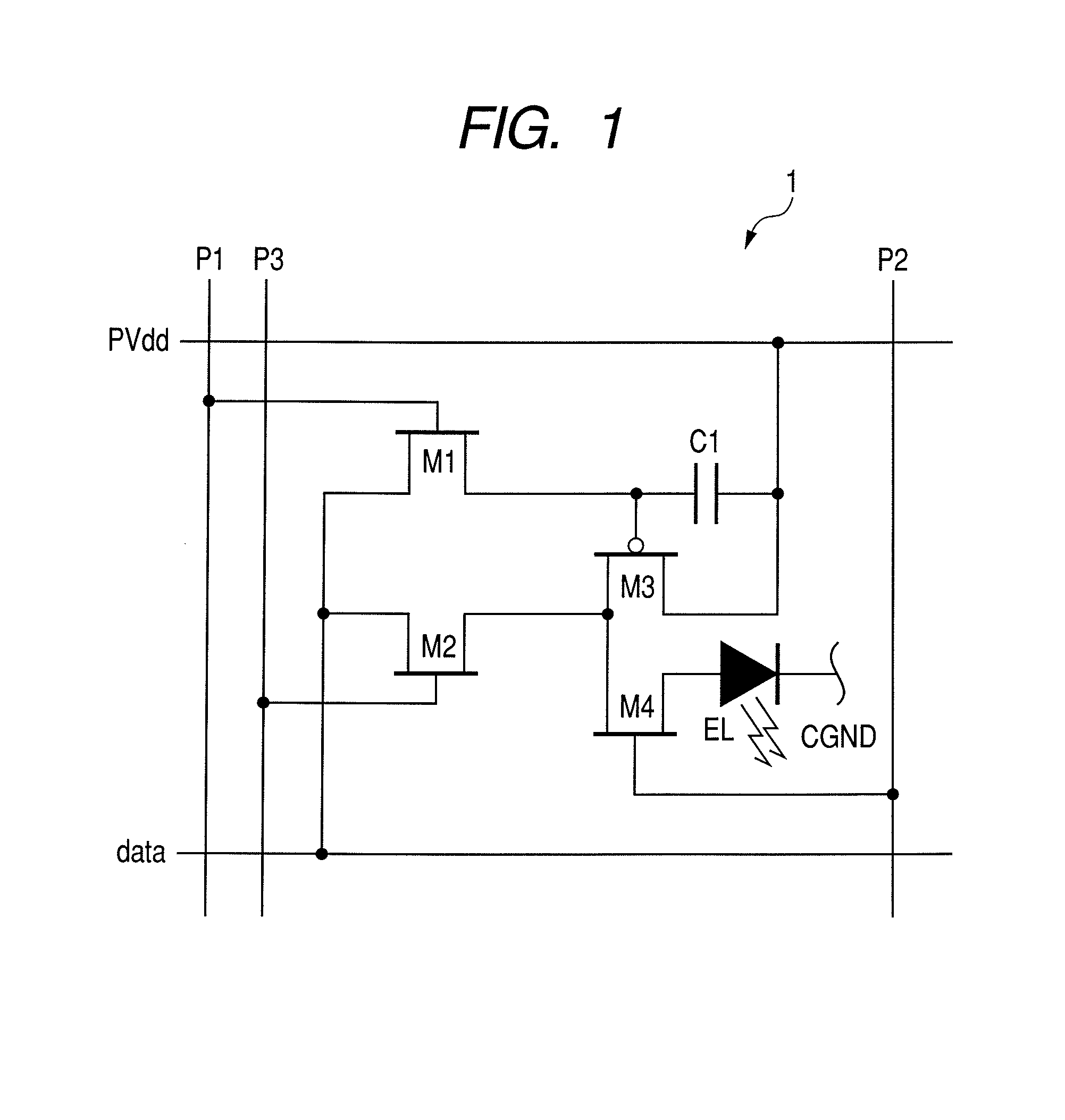
[0043]An EL panel (active matrix type display apparatus) according to the present embodiment shown in FIG. 1 uses the current writing type pixel circuit 1 shown in FIG. 10 as the pixel circuit 1 disposed in a display region 2 of the color EL panel shown in FIG. 8. The pixel circuit 1 shown in the figure includes an EL element (referred to also as [OLED: Organic Light Emitting Diode]) which is a display element two-dimensionally disposed and a drive circuit of the EL element.
[0044]The drive circuit of FIG. 1, as shown in FIG. 8, is disposed at a position where a scanning line 7 and a signal line 4 are intersected, and includes three switch transistors (hereinafter, referred to as first to third transistors) M1, M2 and M4, and a drive transistor M3 capable of injecting the current to the EL element, and a capacitive element (capacitor or holding capacitance) C1....
second embodiment
[Second Embodiment]
[0081]Next, a second embodiment of the present invention will be described with reference to FIG. 4.
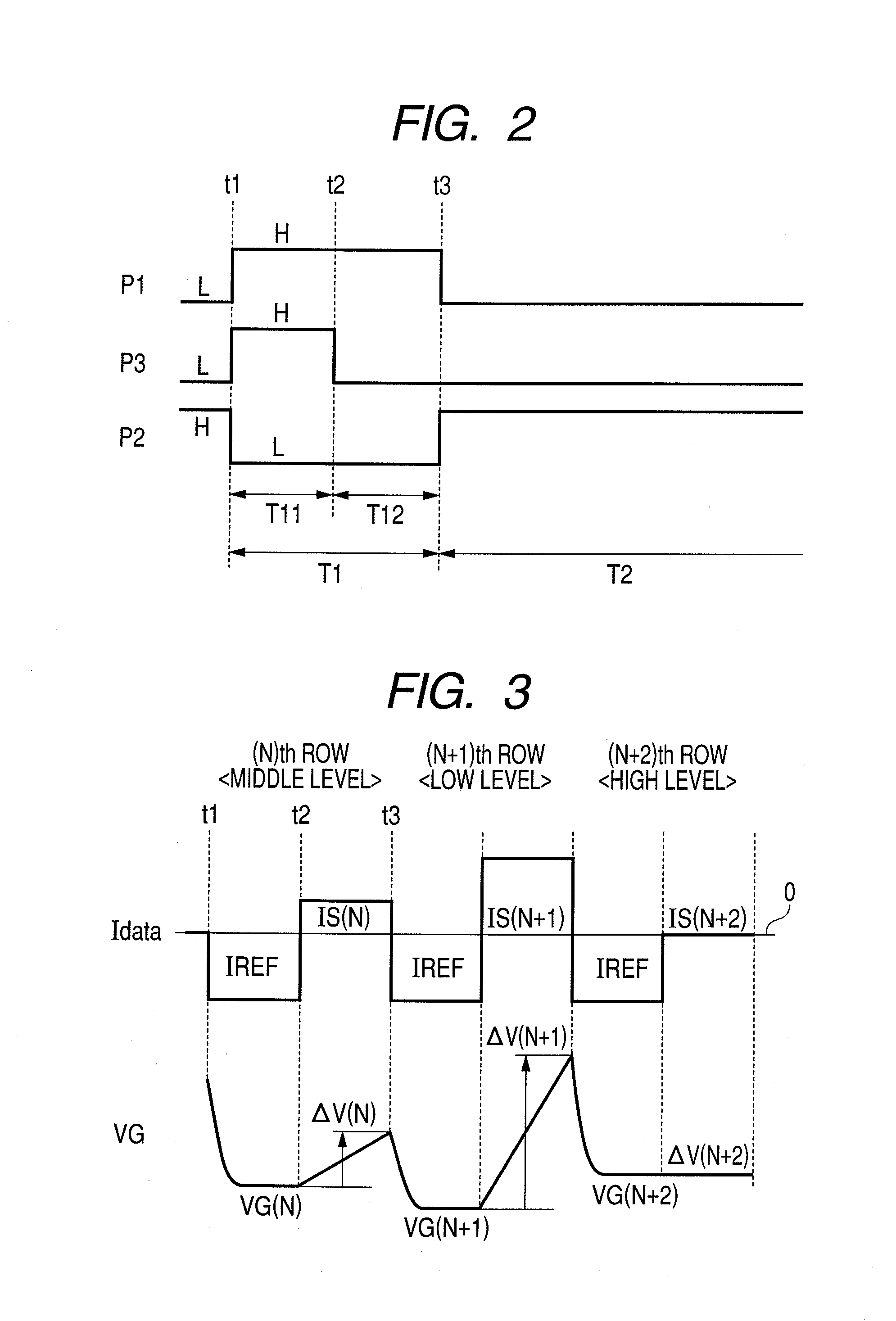
[0082]While the first embodiment applies the pixel circuit of FIG. 10, the present embodiment applies the pixel circuit of FIG. 9. That is, in the present embodiment, a transistor M2 is connected to a signal line “Data” through a transistor M1. Other configurations are the same as those of the first embodiment. A pixel circuit 1 of the present embodiment shown in FIG. 4 can perform the same operation as the pixel circuit 1 of FIG. 1 using each scan signal of scan lines P1, P2 and P3 shown in FIG. 2 and a current “Idata” of a signal line “data” shown in FIG. 3, and can achieve the same effect.
third embodiment
[Third Embodiment]
[0083]Next, the third embodiment of the present invention will be described with reference to FIGS. 5 to 7.
[0084]A pixel circuit 1 of the present embodiment shown in FIG. 5, when compared with the pixel circuit of FIG. 1, is different in that it has no scanning line P3, but has the scanning lines P1 and P2 only, and that transistors M2 and M4 are formed of two transistors M21 and M22, and two transistors M41 and M42, respectively. In the present embodiment, the transistor M21 and M22 include an n-type TFT, and the transistors M41 and M42 include a P-type TFT. The transistor M21 and M41 and the transistor M22 and M42 are controlled by each scanning signal of the scanning lines P1 and P2, respectively. Other configurations are the same as those of the first embodiment.
[0085]The pixel circuit 1 of FIG. 5 can be operated by each scanning signal of the scanning lines P1 and P2 shown in FIG. 6 and the current “Idata” of a signal line “data” shown in FIG. 7. A difference ...
PUM
 Abstract
Description
Claims
Application Information
 - R&D
- Intellectual Property
- Life Sciences
- Materials
- Tech Scout
- Unparalleled Data Quality
- Higher Quality Content
- 60% Fewer Hallucinations
Browse by: Latest US Patents, China's latest patents, Technical Efficacy Thesaurus, Application Domain, Technology Topic, Popular Technical Reports.
© 2025 PatSnap. All rights reserved.Legal|Privacy policy|Modern Slavery Act Transparency Statement|Sitemap|About US| Contact US: help@patsnap.com


