Optical device structure using non-polar GaN substrates and growth structures for laser applications in 481 nm

Active Publication Date: 2012-08-14
KYOCERA SLD LASER INC
View PDF121 Cites 157 Cited by
  • Summary
  • Abstract
  • Description
  • Claims
  • Application Information

AI Technical Summary

Benefits of technology

[0011]The present invention enables a cost-effective optical device for laser applications. In a specific embodiment, the optical device can be manufactured in a relatively simple and cost effective manner. Depending upon the embodiment, the present apparatus and method can be manufactured using conventional materials and / or methods. The present laser device uses a non-polar gallium nitride material capable of achieving a 481 nm light. These and other benefits may be described throughout the present specification and more particularly below by reference to the specification and attached drawings.

Problems solved by technology

Unfortunately, there are several disadvantages to the conventional Edison light bulb.
First, the conventional light bulb dissipates considerable energy as thermal energy.
Secondly, reliability is a concern.
The conventional light bulb routinely fails from thermal expansion and contraction of the filament element.
Another disadvantage is that light bulbs emit light in all directions.
Therefore they are not ideal for applications requiring directionality or focus, such as projection displays, optical data storage, or specialized directed lighting.
In addition, the size, weight, and cost of the lasers were undesirable.
As laser technology evolved, more efficient lamp pumped solid state laser designs were developed for the red and infrared wavelengths, but these technologies remained a challenge for blue and green and blue lasers.
The resulting green and blue lasers were called “lamped pumped solid state lasers with second harmonic generation” (LPSS with SHG) had wall plug efficiency of ˜1%, and were more efficient than Ar-ion gas lasers, but were still too inefficient, large, expensive, fragile for broad deployment outside of specialty scientific and medical applications.
Additionally, the gain crystal used in the solid state lasers typically had energy storage properties which made the lasers difficult to modulate at high speeds which limited its broader deployment.
The change to diode pumping, however, increases the system cost and requires precise temperature control.
The resulting laser is large, consumes substantial power, yet does not address the energy storage properties which make the lasers difficult to modulate at high speeds.
These lasers designs improve the efficiency, cost and size compared to DPSS—SHG lasers, but the specialty diodes and crystals required make this challenging today.
Additionally, while the diode-SHG lasers have the benefit of being directly modulated, they suffer from sensitivity to temperature, limiting their application.

Method used


Image

  • Optical device structure using non-polar GaN substrates and growth structures for laser applications in 481 nm
  • Optical device structure using non-polar GaN substrates and growth structures for laser applications in 481 nm
  • Optical device structure using non-polar GaN substrates and growth structures for laser applications in 481 nm

Examples


embodiment

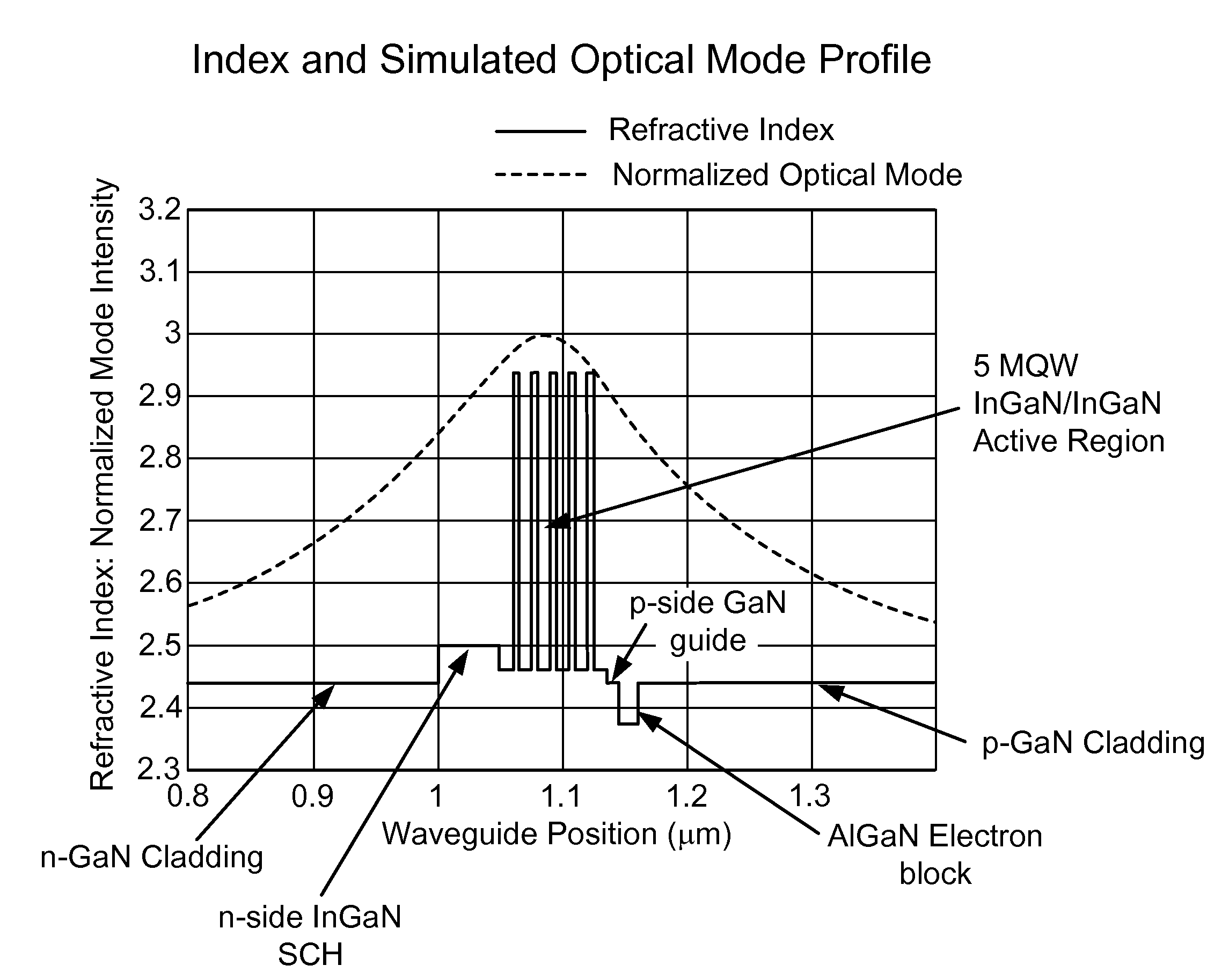
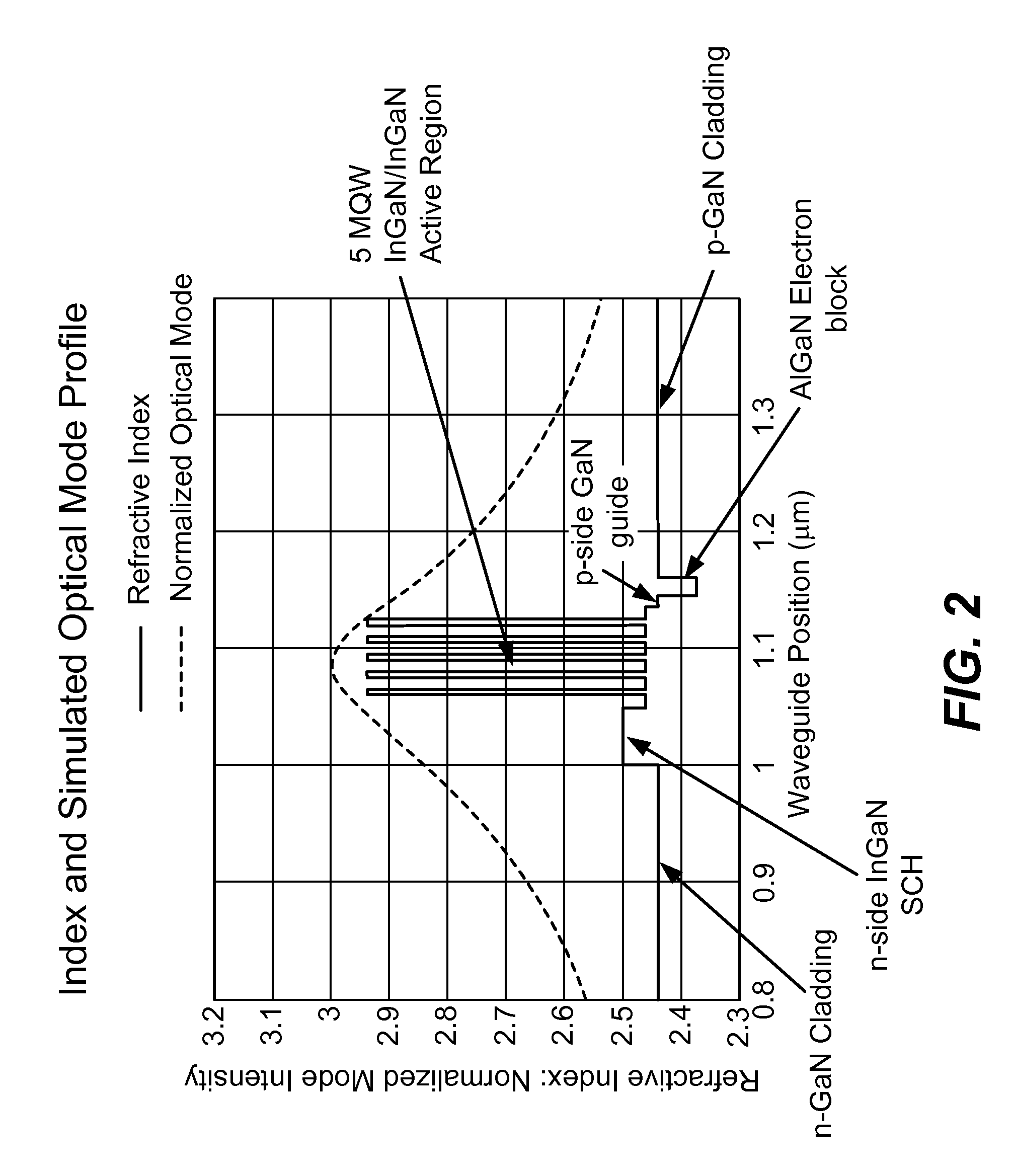
[0031]In a specific embodiment, the present invention provides an alternative device structure capable of emitting 481 nm light, among others, in a ridge laser embodiment. The device is provided with one or more of the following elements, as also referenced in FIGS. 3A and 3B.

[0032]n-GaN cladding layer with a thickness from 100 nm to 3000 nm with Si doping level of 5E17 to 3E18 cm-3

[0033]n-side SCH layer comprised of InGaN with molar fraction of indium of between 4% and 6% and thickness from 45 to 60 nm

[0034]Multiple quantum well active region layers comprised of five 4.5-5.5 nm InGaN quantum wells separated by four 9.5-10.5 nm InGaN barriers with an indium molar fraction of between 1.5% and 3%

[0035]p-side guide layer comprised of GaN with molar a thickness from 10 nm to 20 nm.

[0036]Electron blocking layer comprised of AlGaN with molar fraction of aluminum of between 15% and 22% and thickness from 10 nm to 15 nm and doped with Mg.

[0037]p-GaN cladding layer with a thickness from 400 ...


PUM


Abstract

An optical device. The optical device comprises a GaN substrate having a non-polar surface region, an n-type GaN cladding layer, an n-type SCH layer comprised of InGaN, a multiple quantum-well active region comprised of five InGaN quantum well layers separated by four InGaN barrier layers, a p-type guide layer comprised of GaN, an electron blocking layer comprised of AlGaN, a p-type GaN cladding layer, and a p-type GaN contact layer.

Description

CROSS-REFERENCE TO RELATED APPLICATION[0001]This application claims priority to U.S. Ser. No. 61 / 177,317, filed May 12, 2009; which is commonly assigned and hereby incorporated by reference.BACKGROUND OF THE INVENTION[0002]This invention is directed to optical devices and related methods. More particularly, the invention provides a method and device for emitting electromagnetic radiation using non-polar gallium containing substrates, such as GaN, MN, InN, InGaN, AlGaN, and AlInGaN, and others. By way of example, the invention can be applied to optical devices, lasers, light emitting diodes, solar cells, photoelectrochemical water splitting and hydrogen generation, photodetectors, integrated circuits, and transistors, among other devices.[0003]In the late 1800's, Thomas Edison invented the light bulb. The conventional light bulb, commonly called the “Edison bulb,” has been used for over one hundred years for a variety of applications, including lighting and displays. The conventional...

Claims


Application Information

Patent Timeline
IPC IPC(8): H01L33/00H01L29/06H01L31/00
CPCB82Y20/00H01S5/3202H01S5/34333H01S5/0202H01S5/2009H01S5/2031H01S5/22H01S5/3211H01S5/2201H01S5/32025
Inventor RARING, JAMES W.
Owner KYOCERA SLD LASER INC
Why Eureka
Try Eureka