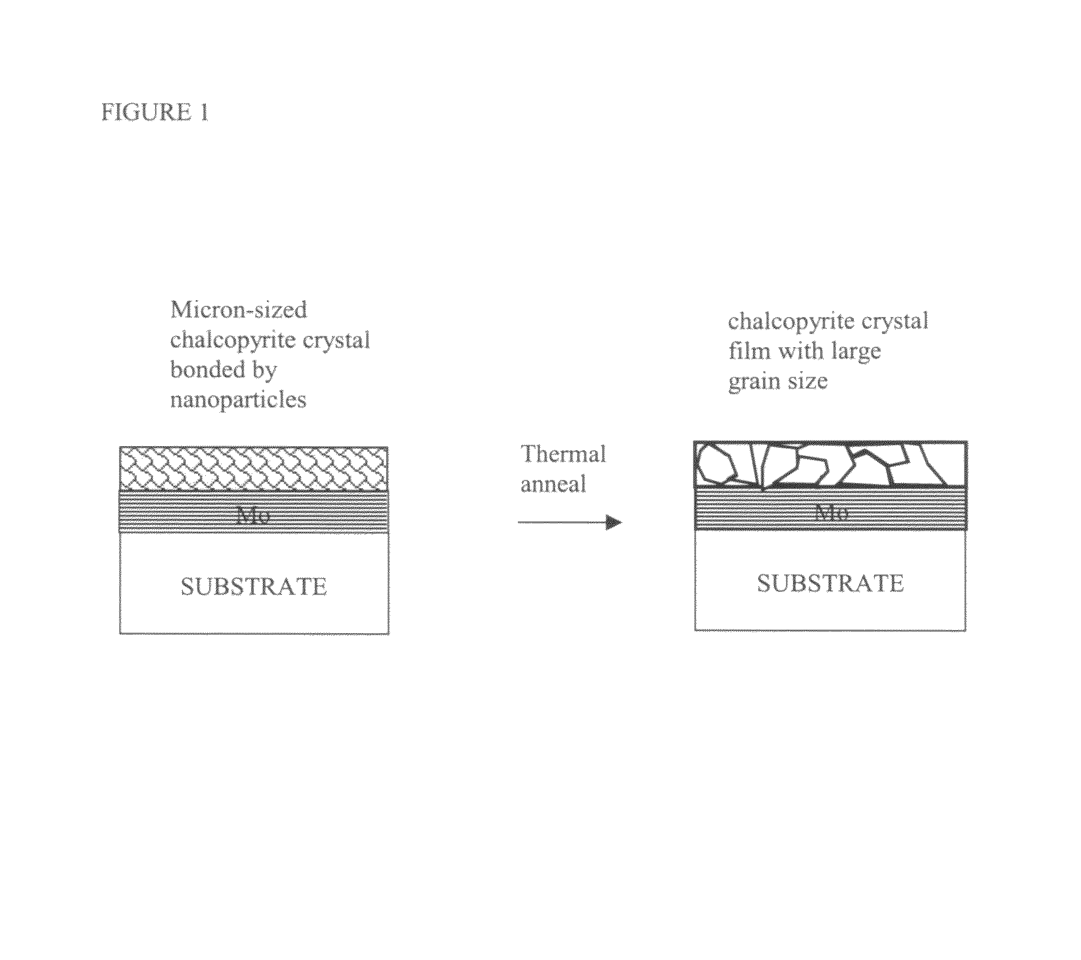
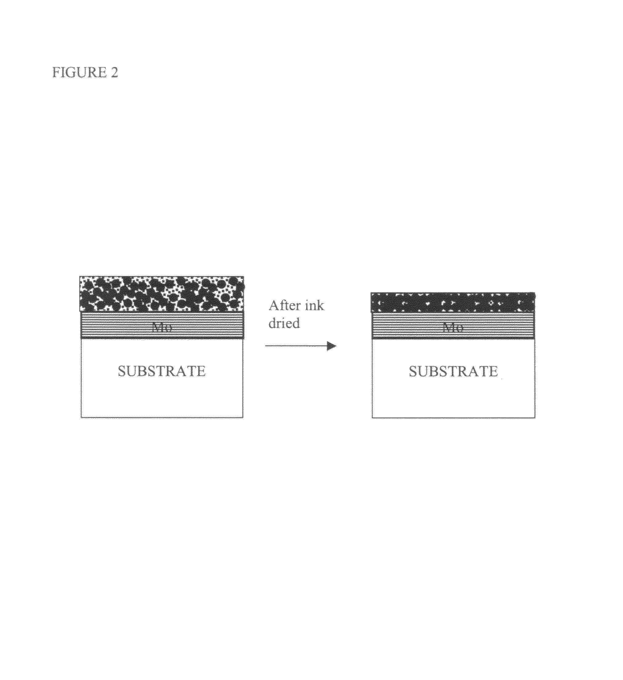
Manufacture of thin solar cells based on ink printing technology
a solar cell and ink printing technology, applied in the field of semiconductive ink compositions, can solve the problems of indium loss, cis modules produced are still too expensive to compete with polycrystalline si based solar modules, and the pve process is difficult to large-scale commercial scale pv production, etc., to achieve high-performance solar cells, increase the open circuit voltage of solar cells, and effectively absorb short-wavelength sunlight
- Summary
- Abstract
- Description
- Claims
- Application Information
AI Technical Summary
Benefits of technology
Problems solved by technology
Method used
Image

Examples
example 1
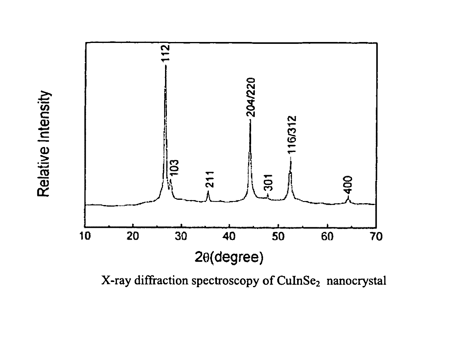
[0043]A Compound semiconductor CuInSe2 was prepared by reacting equivalent mole of Cu powder, indium shots with two mole equivalent amount of selenium pellets at temperature of 350° C. under a pressured nitrogen atmosphere (50 Psi) for 2 hours. The formed CuInSe2 crystal material was crashed into fine power of about 300 μm, and ball milled into micro-sized fine power with the average particle size of about 0.6 μm suspended in mixture solvent of butyl acetate / anisole (1:1 v / v) with the concentration of 40% (g / mL). Thus formed ink is drop-coated on a molybdenum (0.6 μm) coated soda lime glass with the final black film thickness of 2.0 μm upon drying at 160° C. under vacuum. Dektak surface profile shows the film is not smooth with the variation of 30%. The film is further annealed at argon atmosphere at 300° C. for 2 hours, and the film was peeled off by a scotch tape test. No solar cell device was made as the result of loose film morphology.
example 2
[0044]A direct formation of CuInGaSe2 nanoparticle through a chemical reaction in the mixture solvent of dichlorobenzene and trioctyl phosphine was carried out:
Cu(acac)2+In(acac)3++2Se→CuInSe2 (1)
[0045]The formed nanoparticle CIS was purified through a repeated dissolving and precipitation method in dichlorobenzene and ethanol, and finally stabilized in a capping agent, oleylamine. The ink could be used for screen printing, brushing, dipping, spin-coating, ink-jet printing, or rod-coating to form film of CuInSe2 film. By a simple rod-coating on a Mo coated soda lime glass substrate, and dried under vacuum oven at 150° C. for 3 hours, a smooth film (non-uniformity2, with the performance of Voc=0.421 V; Jsc=18.8 mA / cm2, Field effect %=40%; Energy conversion efficiency=3.2%.
example 3
[0046]A CIS semiconductor ink was formulated by combining the following ingredients in a solvent vehicle:
CuInSe2 particles as prepared and ball milled to 0.6 μm size: 60 parts by weight
Nanosized CuInSe2 as prepared in Example 2: 30 parts by weight
Oleyl amine: 3.0 parts by weight
Anisole: 60 parts
Butyl acetate: 60 parts
[0047]By using the above formulated ink, a standard solar cell was made according to the description of Example 2, and the following structure: SLG Glass / Mo (0.6 μm) / CIS 2.0 um / CdS (50 nm) / i-ZnO 60 nm / ZnO:Al (0.5 μm) showed photovoltaic effect under the illumination of 1.5 AM standard condition with the irradiance of 1000 W / m2, with the performance of Voc=0.491 V; Jsc=31.8 mA / cm2, Field effect %=57%; Energy conversion efficiency=9.1%.
PUM
 Abstract
Description
Claims
Application Information
 - R&D
- Intellectual Property
- Life Sciences
- Materials
- Tech Scout
- Unparalleled Data Quality
- Higher Quality Content
- 60% Fewer Hallucinations
Browse by: Latest US Patents, China's latest patents, Technical Efficacy Thesaurus, Application Domain, Technology Topic, Popular Technical Reports.
© 2025 PatSnap. All rights reserved.Legal|Privacy policy|Modern Slavery Act Transparency Statement|Sitemap|About US| Contact US: help@patsnap.com