Communication system using multi-phase clock signals

a communication system and clock signal technology, applied in the field of communication systems, can solve the problems of increasing the size of the clock generator of the receiver, the difficulty of controlling the skew between the clock signal and data, and the noise in the receiver, so as to reduce the jitter noise, delay time, and the effect of reducing the chip size of the receiver

Inactive Publication Date: 2011-09-20
SAMSUNG ELECTRONICS CO LTD
View PDF12 Cites 4 Cited by
  • Summary
  • Abstract
  • Description
  • Claims
  • Application Information

AI Technical Summary

Benefits of technology

[0015]Therefore, in the communication system according to some example embodiments, a jitter noise may be reduced and a delay time to be generated in a phase interpolator may be shorter than a delay time required by a conventional communication system. Furthermore, a chip size of a receiver may be reduced when the receiver is implemented with a semiconductor integrated circuit.

Problems solved by technology

In a memory system using multi-phase clock signals, it is difficult to control skew between a clock signal and data.
Furthermore, in the memory system using the multi-phase clock signals, if the phase-lock operation is performed only in a clock generator of the receiver to lock phases of the data and the clock signal, the clock signal should be delayed by a long delay time through phase interpolation, thereby increasing a size of the clock generator of the receiver and increasing a noise in the receiver.
However, a noise of the sampling clock signal CK_SP generated in the receiver occurs when the first delay time tDL elapses after the noise of the data DATA occurs.
If data are synchronized with multi-phase clock signals in a manner illustrated in FIG. 1, a large jitter noise occurs and a clock generator requires a long delay time for the described synchronization.
Furthermore, a complex circuit, such as a register, is needed for phase interpolation, and a chip size of a semiconductor integrated circuit increases.

Method used


Image

  • Communication system using multi-phase clock signals
  • Communication system using multi-phase clock signals
  • Communication system using multi-phase clock signals

Examples


Embodiment Construction

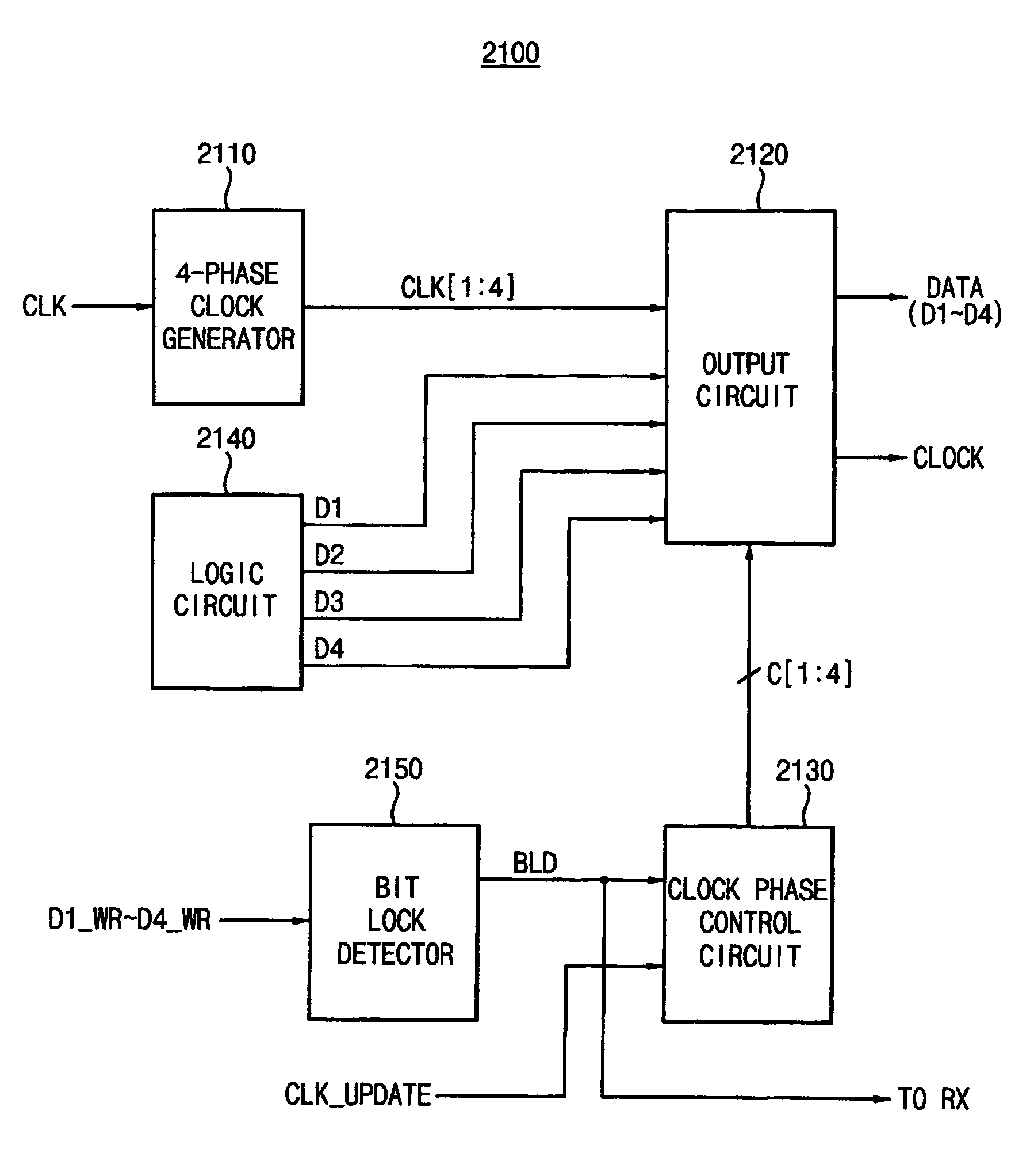
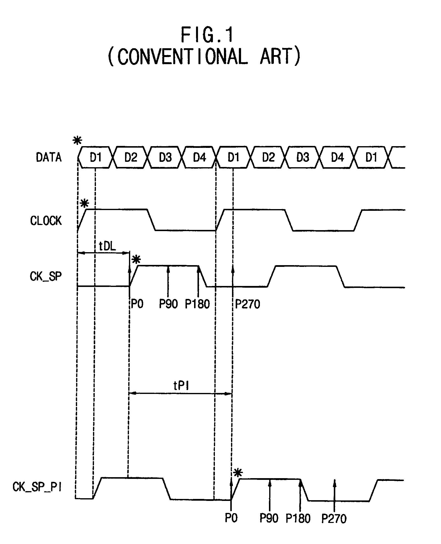
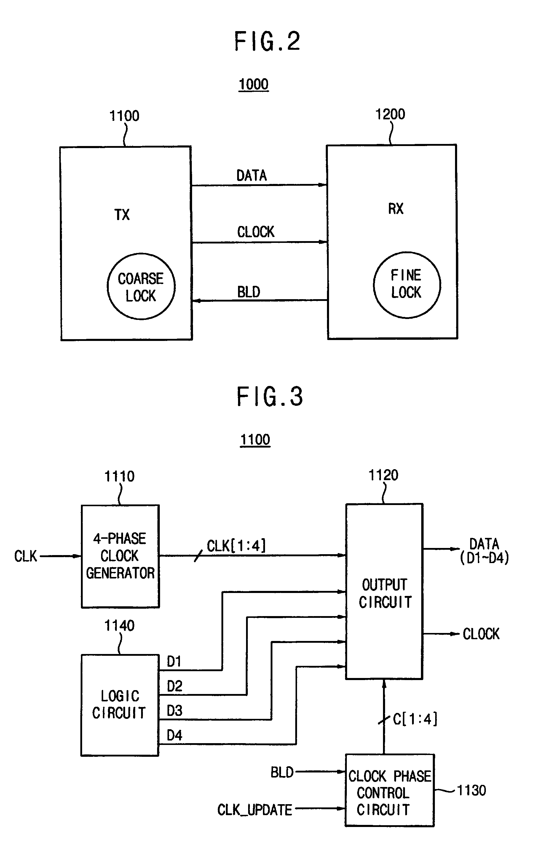
[0031]Embodiments of the present invention now will be described more fully with reference to the accompanying drawings, in which embodiments of the invention are shown. This invention may, however, be embodied in many different forms and should not be construed as limited to the embodiments set forth herein. Rather, these embodiments are provided so that this disclosure will be thorough and complete, and will fully convey the scope of the invention to those skilled in the art. Like reference numerals refer to like elements throughout this application.

[0032]It will be understood that, although the terms first, second, etc. may be used herein to describe various elements, these elements should not be limited by these terms. These terms are used to distinguish one element from another. For example, a first element could be termed a second element, and, similarly, a second element could be termed a first element, without departing from the scope of the present invention. As used herein...


PUM


Abstract

A communication system using multi-phase clock signals. The communication system includes a transmitter and a receiver. The transmitter outputs first data and a clock signal based on first multi-phase clock signals, and performs a coarse lock operation on the clock signal in response to a bit lock detection signal indicating whether or not the first data are bit-locked. The receiver receives the first data and the clock signal from the transmitter, generates second multi-phase clock signals based on the clock signal, generates second data by sampling the first data based on the second multi-phase clock signals, and performs a fine lock operation on the second multi-phase clock signals in response to the bit lock detection signal. Therefore, a jitter noise may be reduced and a size of a multi-phase clock generator included in the receiver may be reduced.

Description

CROSS-REFERENCE TO RELATED APPLICATIONS[0001]This application claims priority under 35 USC §119 to Korean Patent Application No. 2007-48254, filed on May 17, 2007 in the Korean Intellectual Property Office (KIPO), the disclosure of which is incorporated herein in its entirety by reference.BACKGROUND OF THE INVENTION[0002]1. Field of the Invention[0003]The present invention relates to a communication system, and more particularly, to a communication system using multi-phase clock signals.[0004]2. Description of the Related Art[0005]A communication system includes a transmitter and a receiver. The transmitter samples data with a clock signal having a fixed period, and transmits the sampled data. The receiver receives the clock signal as well as the data from the transmitter.[0006]As information technology has been developed, integration density and operation speed of a semiconductor memory device have increased. A single data rate dynamic random access memory (SDR DRAM) outputs data o...

Claims


Application Information

Patent Timeline
Patent Type & Authority Patents(United States)
IPC IPC(8): H03D3/24
CPCG11C7/1051G11C7/106G11C7/1066G11C7/1078G11C7/1087G11C7/1093H04L7/0008H04L7/033H04L7/02
Inventor JANG, YOUNG-CHAN
Owner SAMSUNG ELECTRONICS CO LTD
Why Eureka
Try Eureka