
Multi-bit spin torque transfer magnetoresistive random access memory with sub-arrays

a random access memory and multi-bit spin technology, applied in the field of multi-bit spin torque transfer magnetoresistive random access memory, can solve the problems of increasing chip area and power consumption, and achieve the effects of reducing chip size and power consumption, consuming less chip area, and less power for data access

Active Publication Date: 2016-09-06
QUALCOMM INC
View PDF10 Cites 32 Cited by
  • Summary
  • Abstract
  • Description
  • Claims
  • Application Information

AI Technical Summary

Benefits of technology

The patent text describes a multi-bit STT-M RAM memory that has sub-arrays with different operating parameters for different memory uses. By using a single memory array with these sub-arrays, it can provide faster data access and lower power consumption compared to using separate memory arrays for different memory uses. This results in smaller chip size and lower power consumption.

Problems solved by technology

Maintaining separate memory arrays having different types of memory uses may require added chip area and power usage.

Method used


Image

  • Multi-bit spin torque transfer magnetoresistive random access memory with sub-arrays
  • Multi-bit spin torque transfer magnetoresistive random access memory with sub-arrays
  • Multi-bit spin torque transfer magnetoresistive random access memory with sub-arrays

Examples


Embodiment Construction

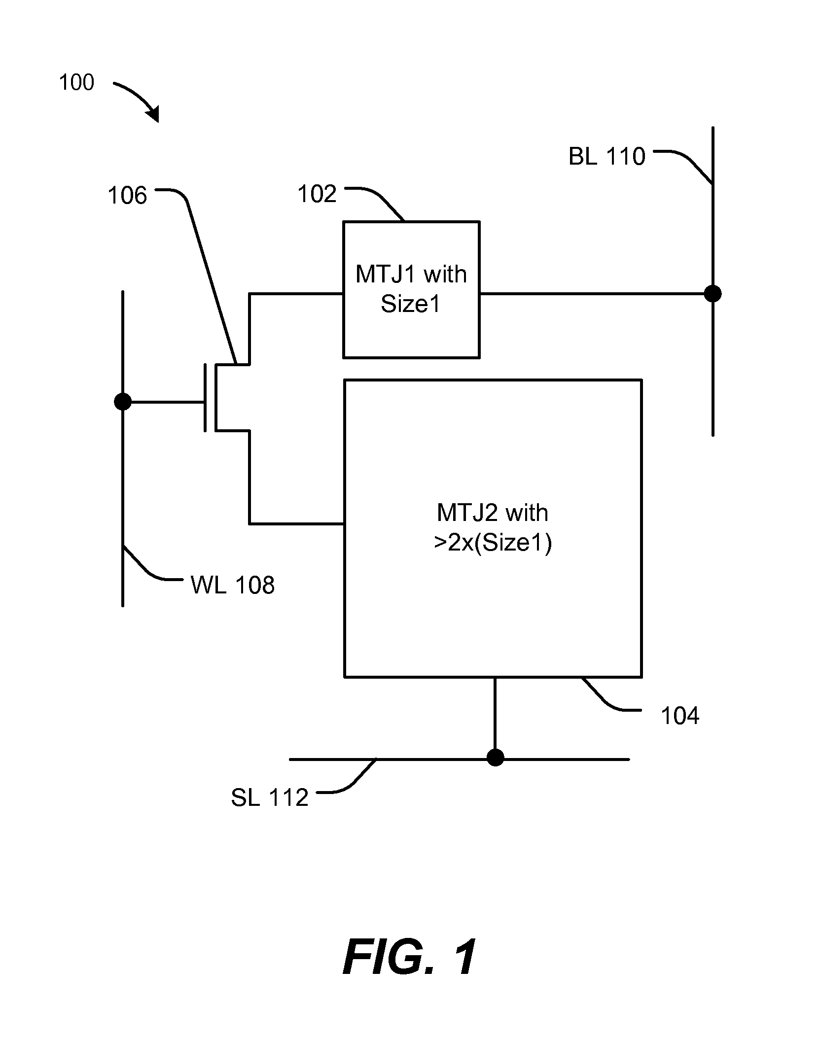
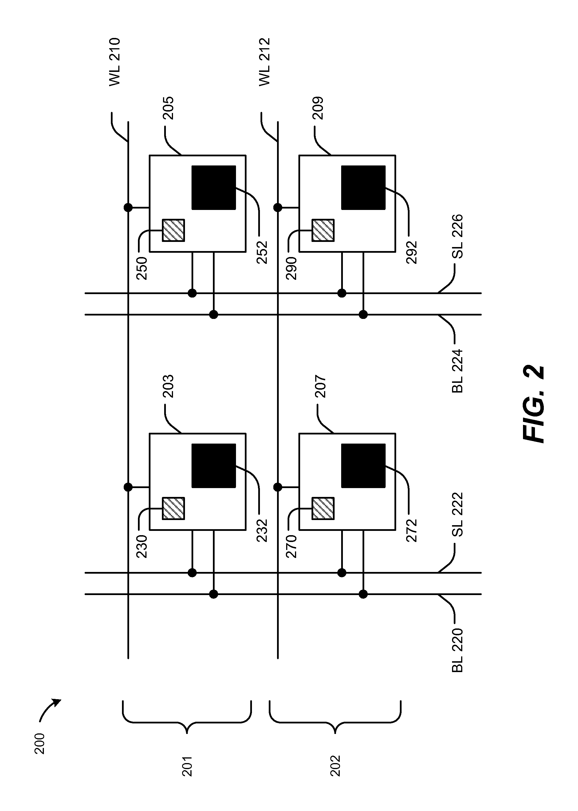
[0021]Referring to FIG. 1, a particular illustrative aspect of a device 100 is shown. The device 100 may be a multi-bit spin torque transfer magnetoresistive random access memory (STT-MRAM) memory cell. The device 100 may be integrated within a die (e.g., a semiconductor die).

[0022]The device 100 includes a first magnetic tunnel junction (MTJ) element 102, a second MTJ element 104, a word line (WL) 108, a bit line (BL) 110, a source line (SL) 112, and an access transistor 106. The first MTJ element 102 is coupled to the bit line 110 and the second MTJ element 104 is coupled to the source line 112.

[0023]The first MTJ element 102 may have a first read margin (AR) that is greater than twice a second read margin of the second MTJ element 104. For example, sizes of the first and second MTJ elements 102, 104 may be associated with particular read margins. Based on the difference in sizes of the MTJ elements 102, 104, the MTJ elements 102, 104 may have operating parameters or characteristi...


PUM


Abstract

A device includes a first magnetic tunnel junction (MTJ) element having a first read margin and a second MTJ element having a second read margin. The first read margin is greater than twice the second read margin. The device also includes an access transistor coupled between the first MTJ element and the second MTJ element. A gate of the access transistor is coupled to a word line. The first MTJ element, the second MTJ element, and the access transistor form a multi-bit spin torque transfer magnetoresistive random access memory (STT-MRAM) memory cell.

Description

I. FIELD[0001]The present disclosure is generally related to a multi-bit spin torque transfer magnetoresistive random access memory (STT-MRAM) with sub-arrays.II. DESCRIPTION OF RELATED ART[0002]Advances in technology have resulted in smaller and more powerful computing devices. For example, a variety of portable personal computing devices including wireless telephones, such as mobile and smart phones, tablets and laptop computers are small, lightweight, and easily carried by users. These devices can communicate voice and data packets over wireless networks. Further, many such devices incorporate additional functionality such as a digital still camera, a digital video camera, a digital recorder, and an audio file player. Also, such devices can process executable instructions, including software applications, such as a web browser application, that can be used to access the Internet. As such, these devices can include significant computing capabilities.[0003]Electronic devices, such ...

Claims


Application Information

Patent Timeline
Patent Type & Authority Patents(United States)
IPC IPC(8): G11C11/00G11C11/16
CPCG11C11/1659G11C11/161G11C11/1673G11C11/5607G06F12/0897
Inventor LU, YULI, XIA
Owner QUALCOMM INC
Learn More