Release layer paste and method of production of a multilayer type electronic device
a multi-layer type, electronic device technology, applied in the direction of fixed capacitor details, other chemical processes, fixed capacitors, etc., can solve the problems of sheet attack phenomenon, short-circuit defects, green sheet and short-circuit defects, etc., to achieve the effect of preventing the electrode layer from being ripped off from the supporting film in a predetermined pattern, and preventing the electrode layer from being eroded
- Summary
- Abstract
- Description
- Claims
- Application Information
AI Technical Summary
Benefits of technology
Problems solved by technology
Method used
Image

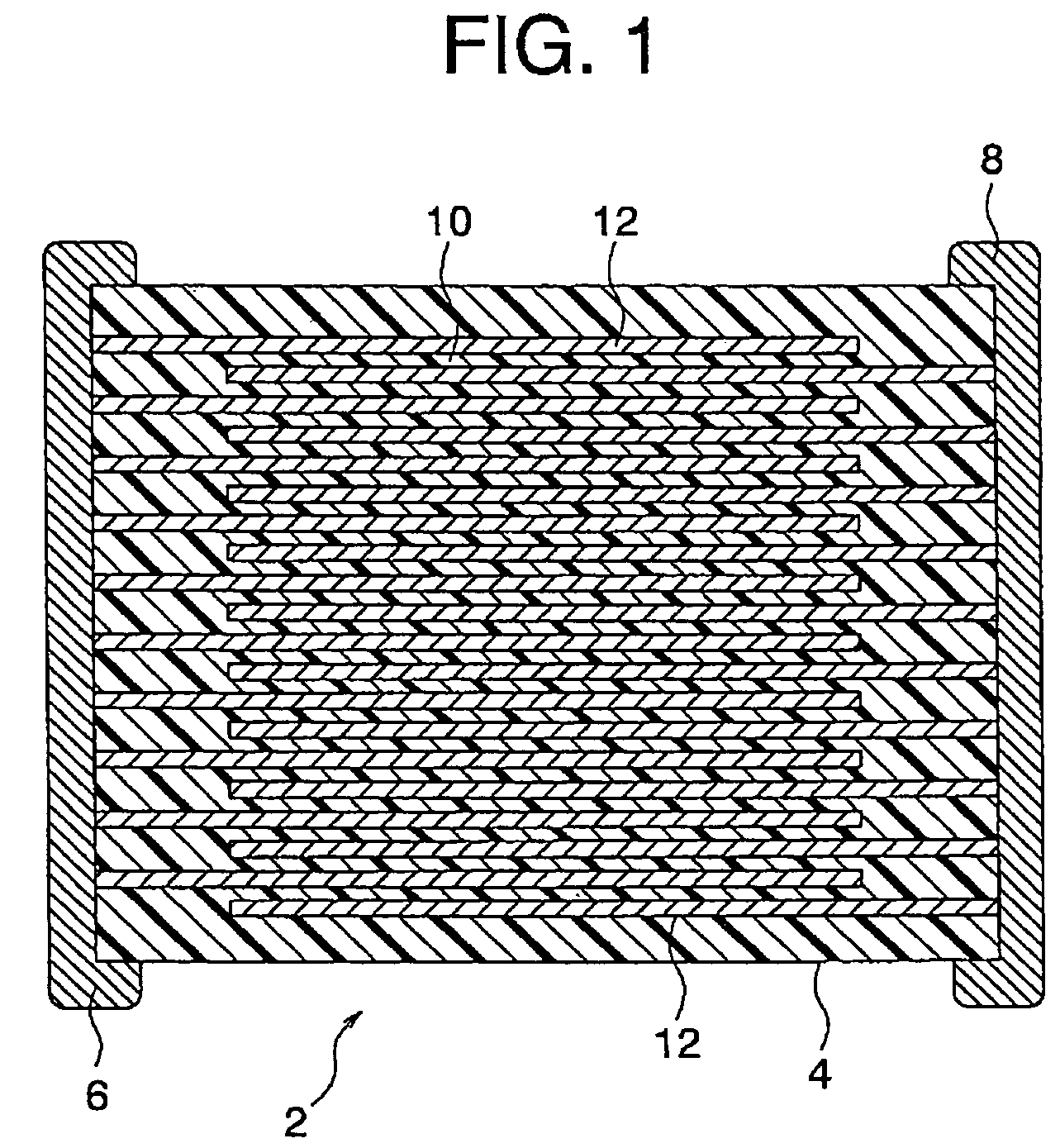
Examples
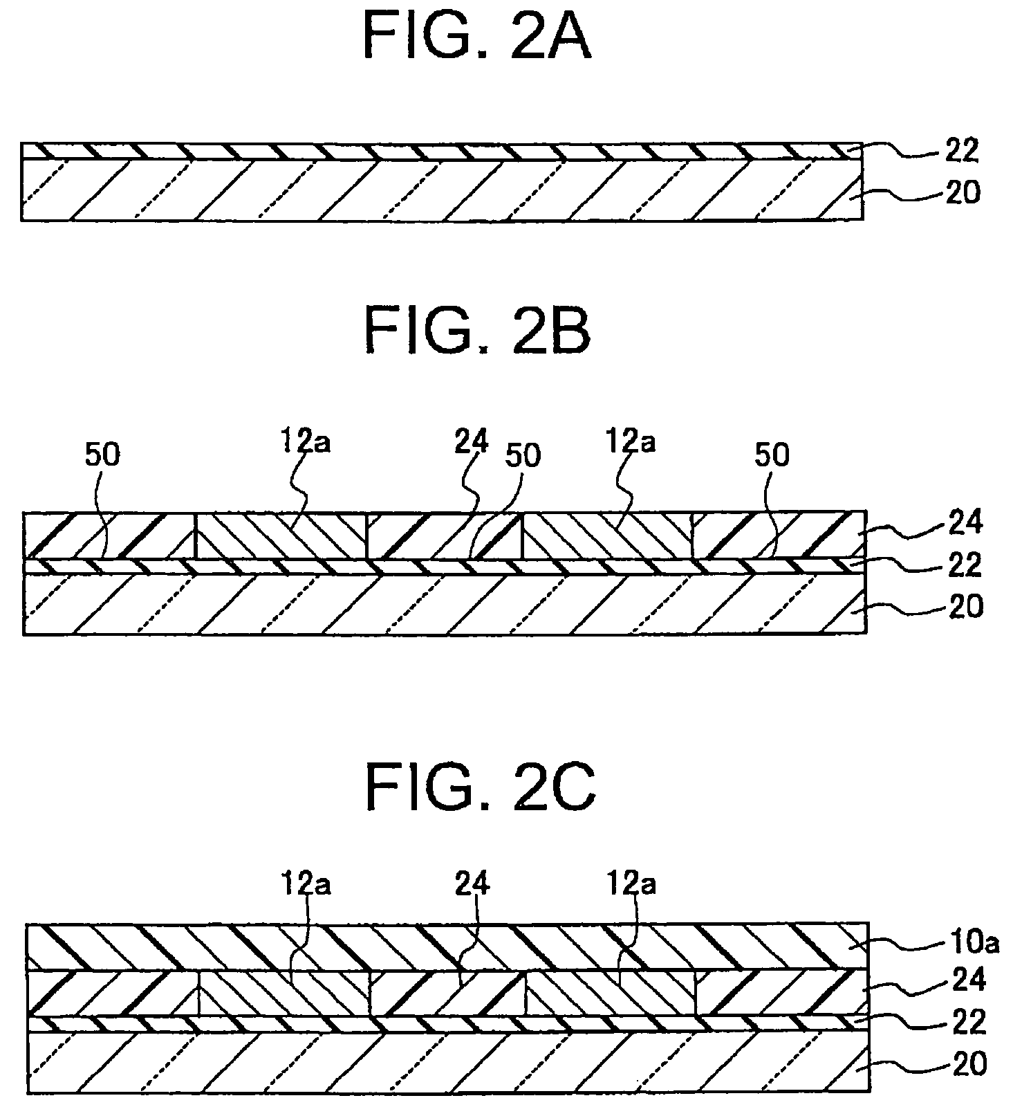
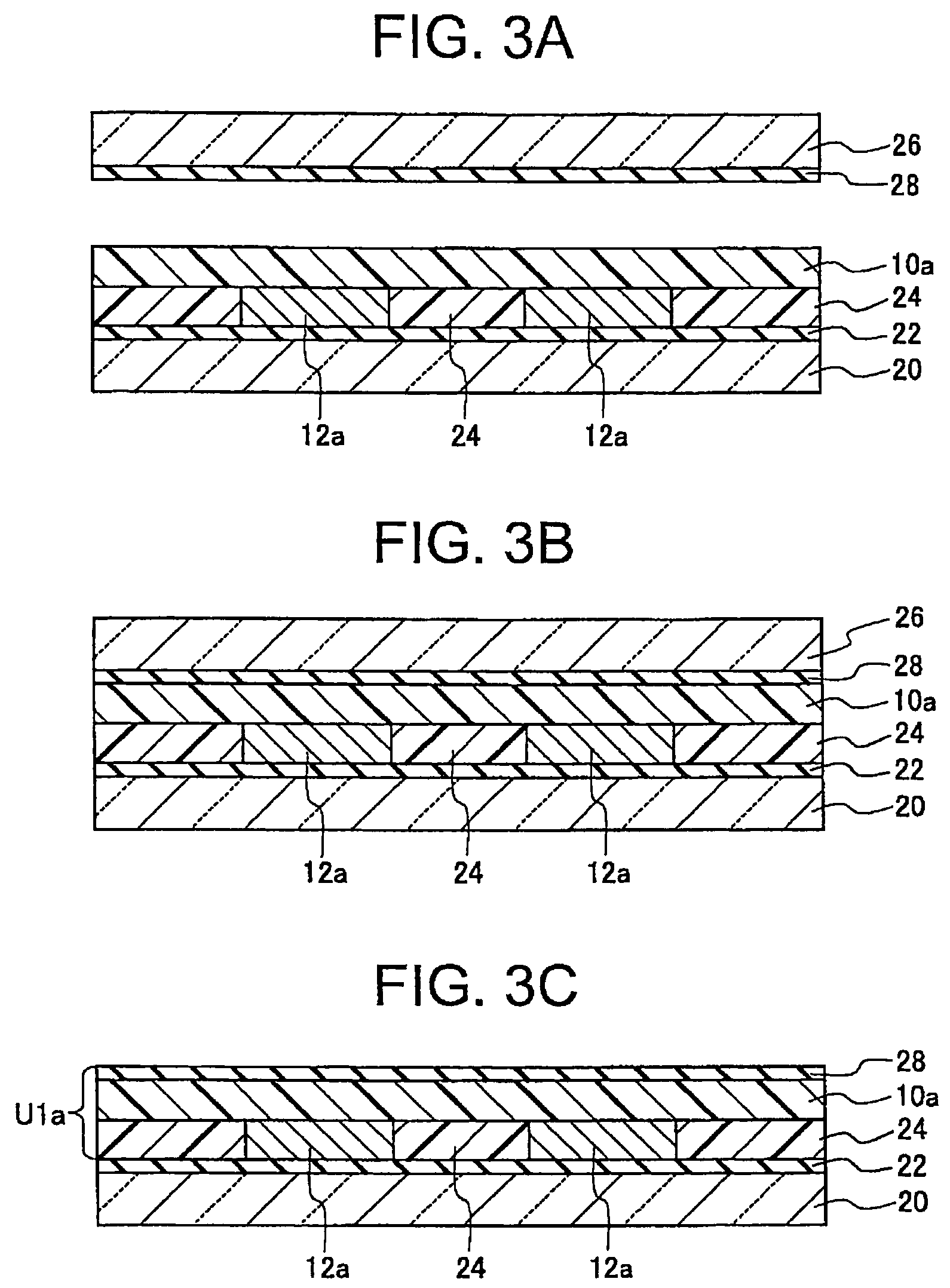
example 1
[0158]Preparation of Release Layer Paste
[0159]Preparation of Additive Slurry
[0160]First, as the additive (subcomponent) materials, (Ba,Ca) SiO3 in an amount of 1.48 parts by weight, Y2O3 in 1.01 parts by weight, MgCO3 in 0.72 part by weight, MnO in 0.13 part by weight, and V2O5 in 0.045 part by weight were prepared. Next, the prepared additive (subcomponent) materials were mixed to obtain the additive (subcomponent) material mixture.
[0161]Next, the additive material mixture in an amount of 8.75 parts by weight was mixed and pulverized with ethyl alcohol in 6.21 parts by weight, n-propanol in 6.21 parts by weight, xylene in 2.19 parts by weight, and a polyethylene glycol-based dispersion agent in 0.09 part by weight using a ball mill to obtain an additive slurry. The mixing and pulverization were performed using a 250 cc polyethylene resin vessel charged with 450 g of 2 mmφ ZrO2 media at a peripheral speed of 45 m / min for 20 hours. The pulverized additive material had a particle size...
example 2
[0199]Except for making the dry thickness of the release layer 0.07 μm, the same procedure was followed as in Example 1 to form and evaluate the release layer. The results are shown in Table 2.
example 3
[0200]Except for making the dry thickness of the release layer 0.05 μm, the same procedure was followed as in Example 1 to form and evaluate the release layer. The results are shown in Table 3.
PUM
| Property | Measurement | Unit |
|---|---|---|
| thickness | aaaaa | aaaaa |
| thickness | aaaaa | aaaaa |
| thicknesses | aaaaa | aaaaa |
Abstract
Description
Claims
Application Information
 - R&D
- Intellectual Property
- Life Sciences
- Materials
- Tech Scout
- Unparalleled Data Quality
- Higher Quality Content
- 60% Fewer Hallucinations
Browse by: Latest US Patents, China's latest patents, Technical Efficacy Thesaurus, Application Domain, Technology Topic, Popular Technical Reports.
© 2025 PatSnap. All rights reserved.Legal|Privacy policy|Modern Slavery Act Transparency Statement|Sitemap|About US| Contact US: help@patsnap.com