
Integrated circuit support structures and their fabrication

a support structure and integrated circuit technology, applied in the direction of printed circuit manufacturing, printed circuit aspects, semiconductor/solid-state device details, etc., can solve the problems of increasing complexity and increasing the number of input/output contacts, increasing the complexity of ics, etc., and achieve the effect of large-scale manufacturing

Active Publication Date: 2009-12-22
ZHUHAI ADVANCED CHIP CARRIERS & ELECTRONICS SUBSTRATE SOLUTIONS TECH
View PDF3 Cites 126 Cited by
  • Summary
  • Abstract
  • Description
  • Claims
  • Application Information

AI Technical Summary

Benefits of technology

The present invention provides a new manufacturing technique for multilayer interconnect support structures that are economical and suitable for large scale manufacture. The technique allows for high yields and excellent planarity and smoothness of the resulting structures. The invention also provides a flat, core-less laminated substrate that can accommodate ICs using Flip Chip assembly processes. The substrate has high reliability and can be supplied in single unit format or in multiple unit format. The technique involves the steps of selecting a base layer, depositing layers of conductive and insulating materials, applying an insulating polymeric layer, etching away the first base layer, and depositing a second base layer. The invention also provides a method for fabricating a flat, core-less laminated substrate with multiple layers of conductive and insulating materials.

Problems solved by technology

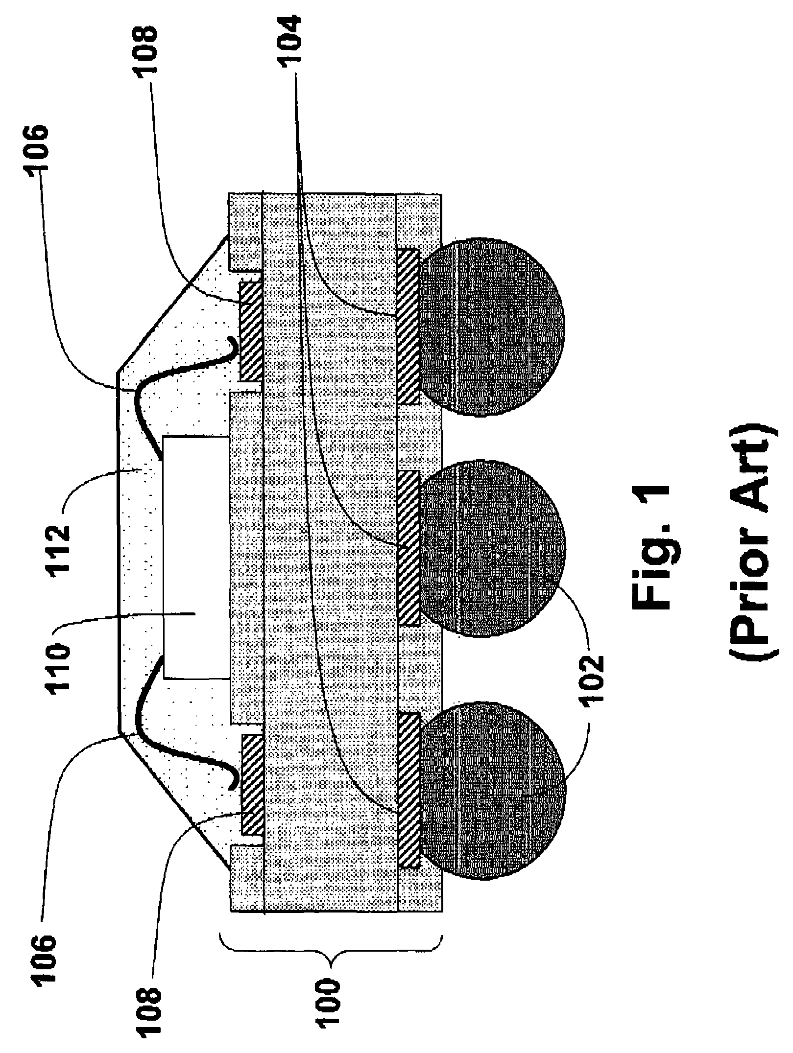
There is a trend towards ever increasing complexity and ever greater miniaturization in the electronics industry.
As such, ICs are becoming more and more complex, and include ever larger numbers of transistors, requiring increasing numbers of input / output contacts.
They are required to operate at ever increasing switching speeds and frequencies, have ever increasing power consumptions and consequently generate ever increasing amounts of heat that requires dissipation.
This is difficult to achieve if the built-up section of the substrate is only formed on one side of the core.
There is a cost to building up layers on both sides of the core however.
It adds more manufacturing process steps which increases fabrication costs.
Since the resulting substrate structure is more complicated, manufacturing yields drop off.
Furthermore, the substrate thickness is increased, resulting in less compact, thicker packages that are less desirable for mobile communication and other applications where miniaturization is required.
This deteriorates the over-all performance of the IC.
PTHs which are fairly expensive to fabricate.
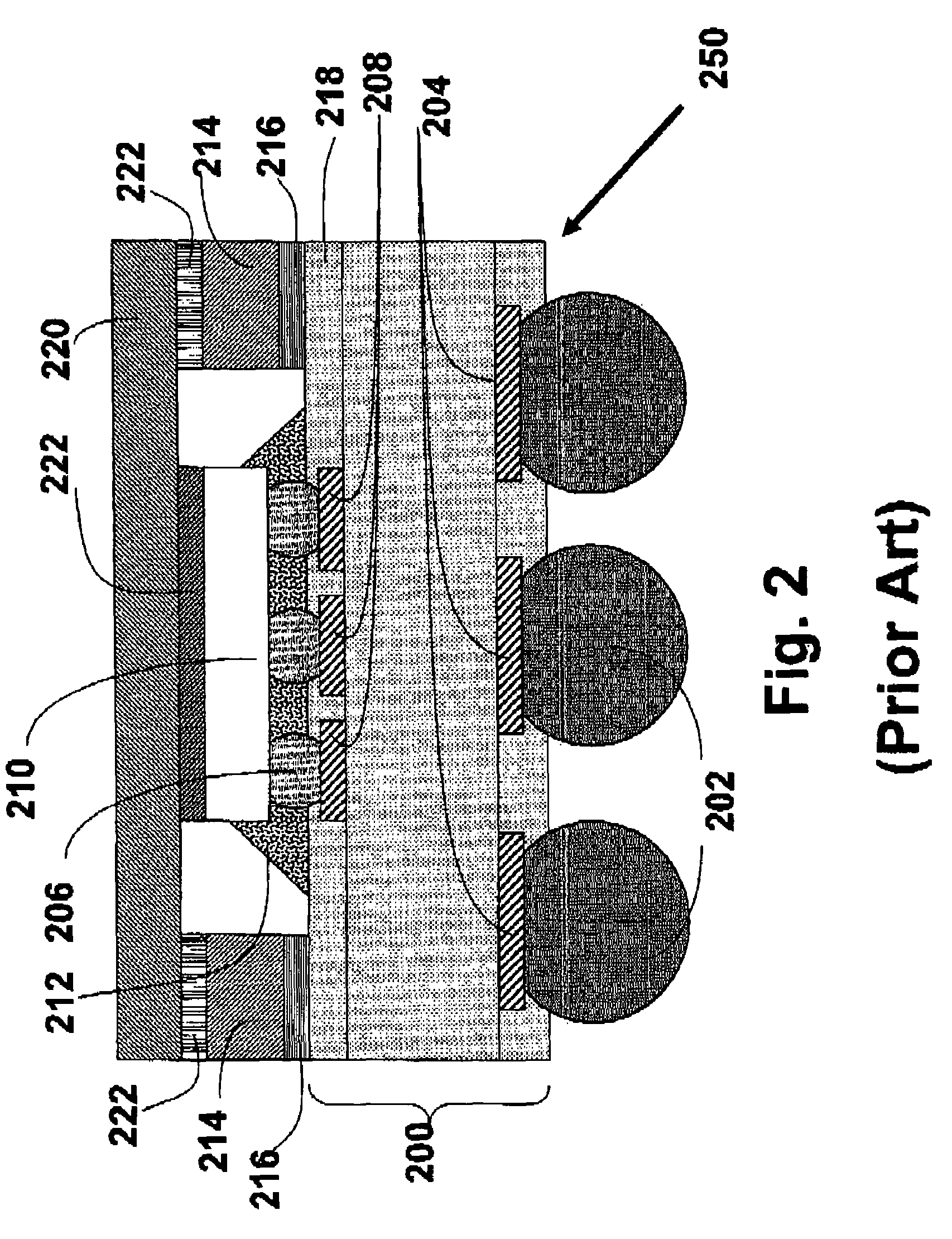
While the above referenced publication apparently introduces a viable methodology for obtaining a core-less substrate, it nevertheless suffers from a number of drawbacks.
Firstly, all the conductor layers of the substrate require expensive thin film interconnects.
While such thin film interconnect conductor layers provide better performance due to their improved densities and finer pitches, they are inappropriate to the substrate's power and ground metal planes which are usually low in density and pitch, and building them using expensive thin film technology is cost prohibitive.
Secondly, these layers usually require a certain metal thickness to reduce electrical resistance and to prevent overheating.
This can become difficult to achieve when using thin film processing techniques.
Thirdly, the Flip Chip bonding process applies a pressure which thin (film interconnect structures are ill equipped to withstand.
Such pressures tend to distort and / or stretch the interconnect structure, which in thin films are typically less then 100 microns thick, and sometimes cause cracking of the thin film dielectric layers which may lead to operating failure of the IC.
Fourthly, it will be appreciated that the presence of a metal stiffener adjacent to the IC consumes valuable space on the external surface of the substrate and may limit usage in applications requiring passive components, such as decoupling capacitors, in close proximity to the IC.
Fifthly, the large aperture metal stiffener used may make this technology unsuitable for applications requiring, for example, multi chip substrates, low body-sized substrates, substrates supplied, for IC assembly, in two dimensional matrix arrays or in strip formats.
Nevertheless, it still suffers from all the drawbacks of the structure of USSN 2002 / 0001937 as detailed above.
Such laminate structures have been found to be susceptible to warping, particularly in consequence of hot pressing or curing processes.
Core-less substrates obtained thereby, typically lack the flatness required for securely and reliably mounting ICs thereupon.
Where such structures have been built up on one side of a metal carrier base that is subsequently removed prior to IC assembly, or thinned down to provide a stiffener supported substrate, internal unbalanced stresses invariably develop during fabrication.
These stresses may he released on removal of the metal carrier, causing substrate curvature and warping.
This can result in poor yields when assembling the IC thereupon, and may even lead to non flat packages that cannot then be mounted onto the corresponding PCB.
Nevertheless, the technology described in U.S. Pat. No. 6,913,814 to Ho et al. has two major drawbacks: Firstly, in order to construct a structure having a bottom layer with a low pitch BGA (hereupon for attachment to a PCB and a high pitch upper IC side, the substrate must be constructed from individual laminae, each having different densities and different dielectric layer thicknesses.
Once again this results in an unbalanced, asymmetrical, structure with an inherent tendency to curving.
Secondly, as is well known to those experienced in the art, connecting the substrate layers with via-to-pad contacts based upon metal contacts achieved through dielectric materials lamination is unreliable for high performance ICs applications, since these have a tendency towards loss of via contact and resultant package failures.
This is especially of concern where high temperature processes are used during IC mounting onto the substrate.

Method used


Image

  • Integrated circuit support structures and their fabrication
  • Integrated circuit support structures and their fabrication
  • Integrated circuit support structures and their fabrication

Examples


Embodiment Construction

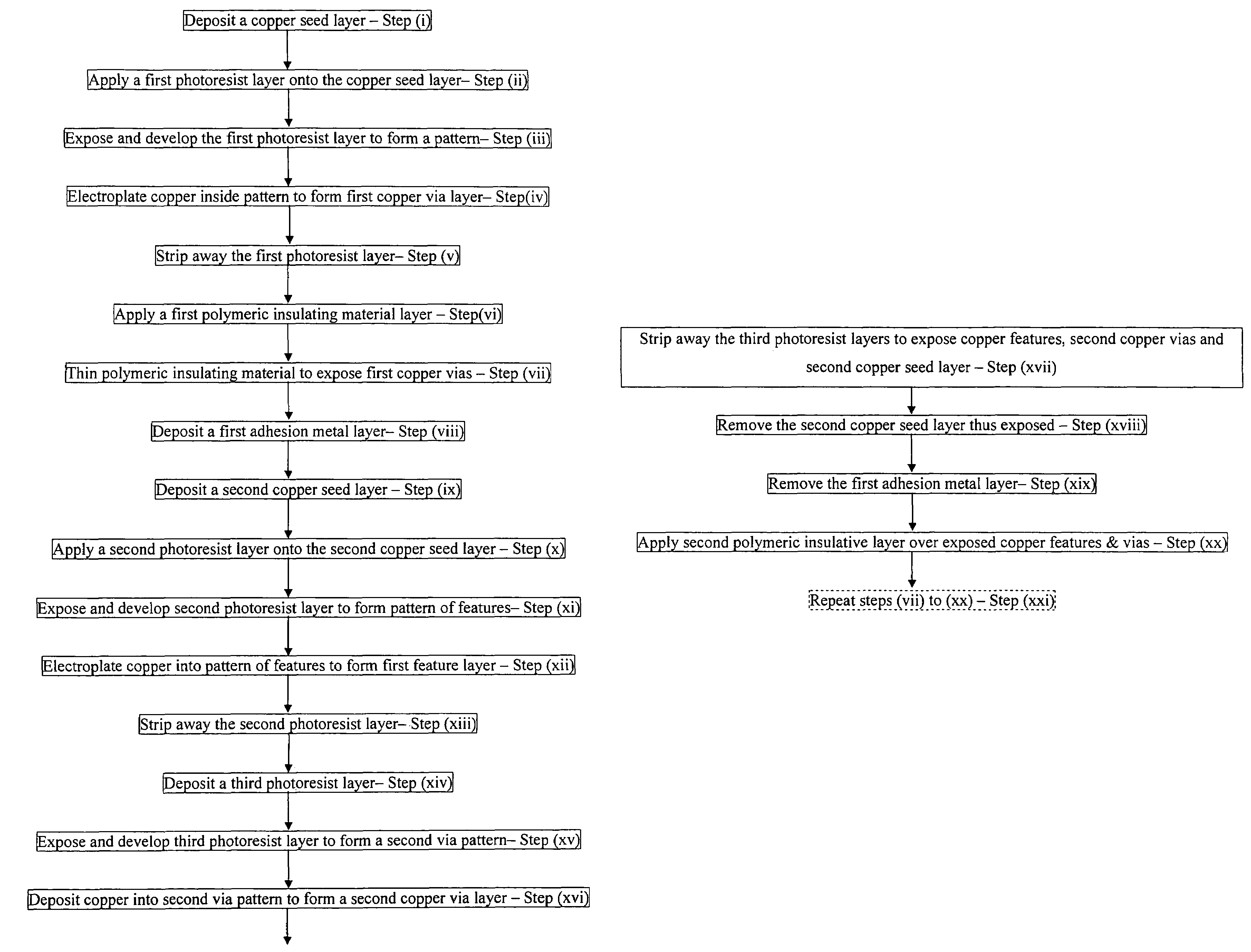
[0160]The present invention relates to a novel processing method for fabricating electronic substrates and to the novel substrates obtainable by that method. Some of the fabrication steps, such as the steps or deposition of photoresist, its exposure and subsequent removal are not described herein in any detail since the various alternative materials and processing routes are well known, and their detailing will render this description unnecessarily cumbersome. Suffice to say, when designing a specific process for a specific product, persons of the art will make appropriate selections from the various alternative materials and processing routes using well established considerations based on parameters such as batch size, substrate complexity and component resolution. Furthermore the actual architecture of the substrate is not described as a general method is provided that may be used to produce a variety of end products. What is described hereinbelow is a method for fabricating multi...


PUM


Abstract

A method of fabricating an electronic substrate comprising the steps of; (A) selecting a first base layer; (B) depositing a first etchant resistant barrier layer onto the first base layer; (C) building up a first half stack of alternating conductive layers and insulating layers, the conductive layers being interconnected by vias through the insulating layers; (D) applying a second base layer onto the first half stack; (F) applying a protective coating of photoresist to the second base layer; (F) etching away the first base layer; (G) removing the protective coating of photoresist; (H) removing the first etchant resistant barrier layer; (I) building up a second half stack of alternating conductive layers and insulating layers, the conductive layers being interconnected by vias through the insulating layers, wherein the second half stack has a substantially symmetrical lay up to the first half stack; (J) applying an insulating layer onto the second hall stack of alternating conductive layers and insulating layers, (K) removing the second base layer, and (L) terminating the substrate by exposing ends of vias on outer surfaces of the stack and applying terminations thereto.

Description

FIELD OF THE INVENTION[0001]The present invention is directed to providing a support structure for integrated circuits, and to methods for the manufacture thereof.BACKGROUND[0002]There is a trend towards ever increasing complexity and ever greater miniaturization in the electronics industry. Space is at a premium, particularly in mobile equipment such as cellular phones and portable computers.[0003]integrated Circuits (ICs) are the heart of these electronic systems. As such, ICs are becoming more and more complex, and include ever larger numbers of transistors, requiring increasing numbers of input / output contacts. They are required to operate at ever increasing switching speeds and frequencies, have ever increasing power consumptions and consequently generate ever increasing amounts of heat that requires dissipation.[0004]ICs are connected to power supplies, user interfaces and other components via printed circuit boards (PCBs). To facilitate the connection of the IC to the PCB, it...

Claims


Application Information

Patent Timeline
Patent Type & Authority Patents(United States)
IPC IPC(8): H01L21/44
CPCH01L21/4857H05K3/4647H05K3/4682H01L2224/48227H01L2224/48091H01L2224/48228H01L2224/73253H01L2924/0102H01L2924/01046H01L2924/01078H01L2924/01079H01L2924/09701H01L2924/15311H01L2924/16195H01L2924/3011H05K3/108H05K3/205H05K3/388H05K3/423H05K2201/096H05K2203/0152H05K2203/0384H05K2203/0733H01L2224/16H01L2924/30107H01L2924/01019H01L2924/01067H01L2224/48465H01L2224/32225H01L2224/73204H01L2224/16225H01L2924/00014H01L2924/00H01L2224/73265H01L2924/181H01L2924/00012H01L23/48H01L23/52
Inventor HURWITZ, DRORFARKASH, MARDECHAYIGNER, EVAZEIDLER, AMITSTATNIKOV, BORISMICHAELI, BENNY
Owner ZHUHAI ADVANCED CHIP CARRIERS & ELECTRONICS SUBSTRATE SOLUTIONS TECH
Learn More