
Integration of high-voltage devices and other devices

Inactive Publication Date: 2009-12-15
QORVO US INC
View PDF6 Cites 22 Cited by
  • Summary
  • Abstract
  • Description
  • Claims
  • Application Information

AI Technical Summary

Benefits of technology

[0005]Embodiments of the present invention relate to integrating high-voltage devices with other circuitry on a semiconductor wafer, which may be fabricated using low-voltage foundry technology, such as a low-voltage complementary metal oxide semiconductor (LV-CMOS) process. The other circuitry may include low-voltage devices, such as switching transistors used in logic circuits, computer circuitry, and the like, or othe

Problems solved by technology

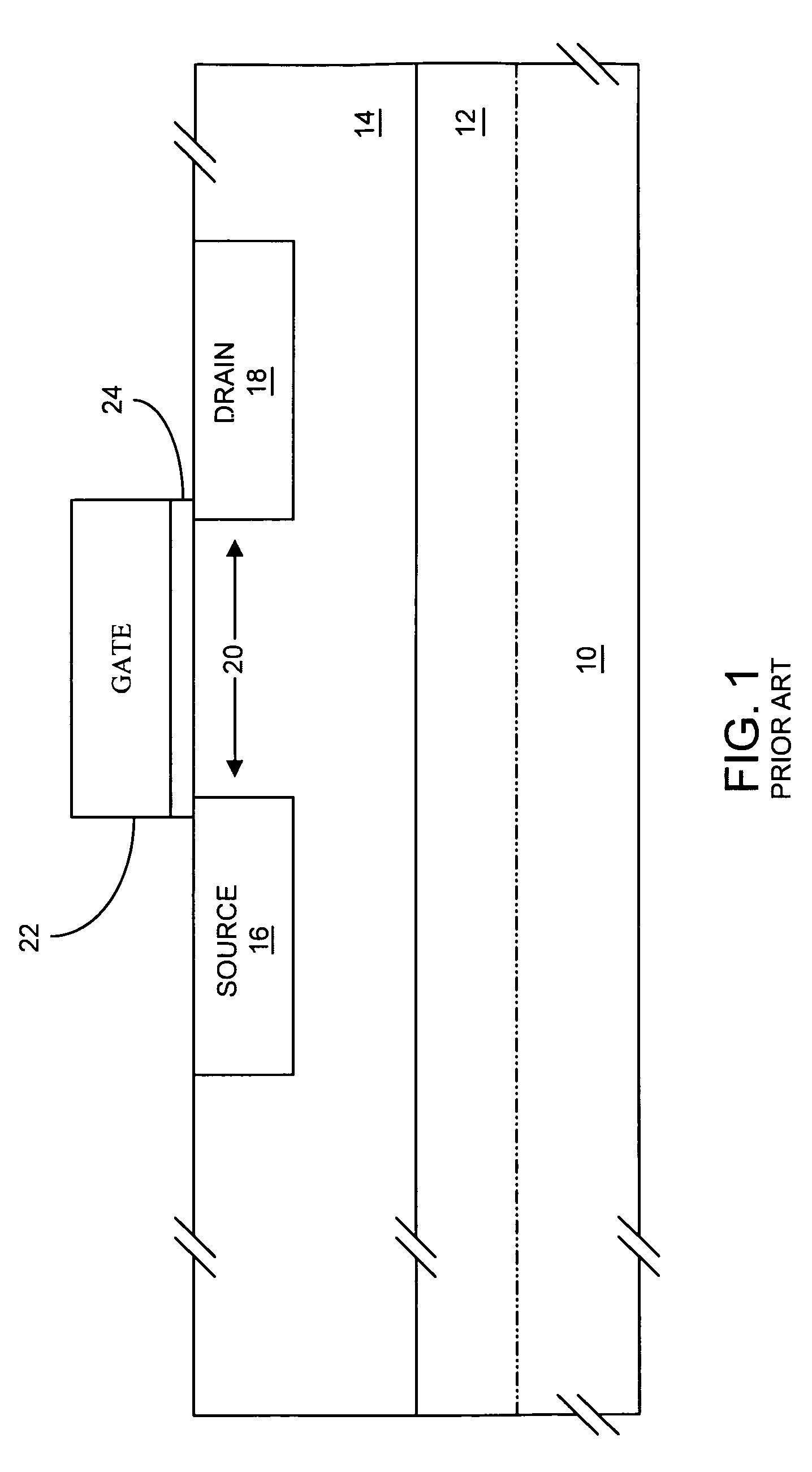
Increases in densities tend to drive down operating voltages, and semiconductor fabrication processes have evolved toward lower operating voltage processes; however, certain applications require relatively high operating voltages.

Method used


Image

  • Integration of high-voltage devices and other devices
  • Integration of high-voltage devices and other devices
  • Integration of high-voltage devices and other devices

Examples


Embodiment Construction

[0037]The embodiments set forth below represent the necessary information to enable those skilled in the art to practice the invention and illustrate the best mode of practicing the invention. Upon reading the following description in light of the accompanying drawing figures, those skilled in the art will understand the concepts of the invention and will recognize applications of these concepts not particularly addressed herein. It should be understood that these concepts and applications fall within the scope of the disclosure and the accompanying claims.

[0038]The present invention relates to integration of lateral high-voltage devices, such as a lateral high-voltage metal oxide semiconductor field effect transistor (LHV-MOSFET), a lateral high-voltage diode (LHVD), a lateral high-voltage thyristor, or any combination thereof, with other circuitry on a semiconductor wafer, which may be fabricated using low-voltage foundry technology, such as a low-voltage complementary metal oxide...


PUM


Abstract

Integrating high-voltage devices with other circuitry, which may be fabricated on a semiconductor wafer using low-voltage foundry technology, such as a low-voltage complementary metal oxide semiconductor (LV-CMOS) process. The other circuitry may include low-voltage devices, such as switching transistors used in logic circuits, computer circuitry, and the like, or other high-voltage devices, such as a microelectromechanical system (MEMS) switch. The high-voltage devices may be used to create useful high-voltage circuits, such as level-shifting circuits, input protection circuits, charge pump circuits, switching circuits, latch circuits, latching switch circuits, interface circuits, any combination thereof, or the like. The high-voltage circuits may be controlled by the other circuitry.

Description

[0001]This application is related to U.S. patent application Ser. No. 12 / 140,491 entitled INTEGRATED LATERAL HIGH-VOLTAGE METAL OXIDE SEMICONDUCTOR FIELD EFFECT TRANSISTOR filed Jun. 17, 2008, and U.S. patent application Ser. No. 12 / 140,504 entitled INTEGRATED LATERAL HIGH-VOLTAGE DIODE AND THYRISTOR filed Jun. 17, 2008, which are concurrently filed herewith and incorporated herein by reference in their entireties.FIELD OF THE INVENTION[0002]The present invention relates to integration of high-voltage devices, such as high-voltage field effect transistors, high-voltage diodes, and high-voltage thyristors, with other circuitry on semiconductor wafers.BACKGROUND OF THE INVENTION[0003]As semiconductor wafer fabrication evolves, device geometries become smaller, which provides greater densities that drive down costs, decrease device sizes, increase functionalities, enable increasing levels of integration, or any combination thereof. Increases in densities tend to drive down operating vo...

Claims


Application Information

Patent Timeline
IPC IPC(8): H01L29/74H01L29/423H01L29/45
CPCH01L29/1045H01L29/7436H03K19/017545H01L29/7835H01L29/861H03K3/352H01L29/7833H01L29/42364
Inventor KERR, DANIEL CHARLESDENING, DAVID C.COSTA, JULIO
Owner QORVO US INC
Learn More