Precisely positioned nanowhiskers and nanowhisker arrays and method for preparing them
a nanowhisker array and precise positioning technology, applied in the direction of nanoinformatics, polycrystalline material growth, condensed vapor, etc., can solve the problems of inability to precisely position nanowhiskers, difficult to control size and surface coverage separately, and in general unsatisfactory for producing a structure with nanowhiskers sufficiently precisely positioned for electronics/photonics components
- Summary
- Abstract
- Description
- Claims
- Application Information
AI Technical Summary
Benefits of technology
Problems solved by technology
Method used
Image
Examples
example 1
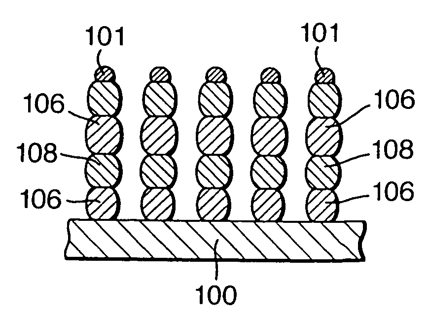
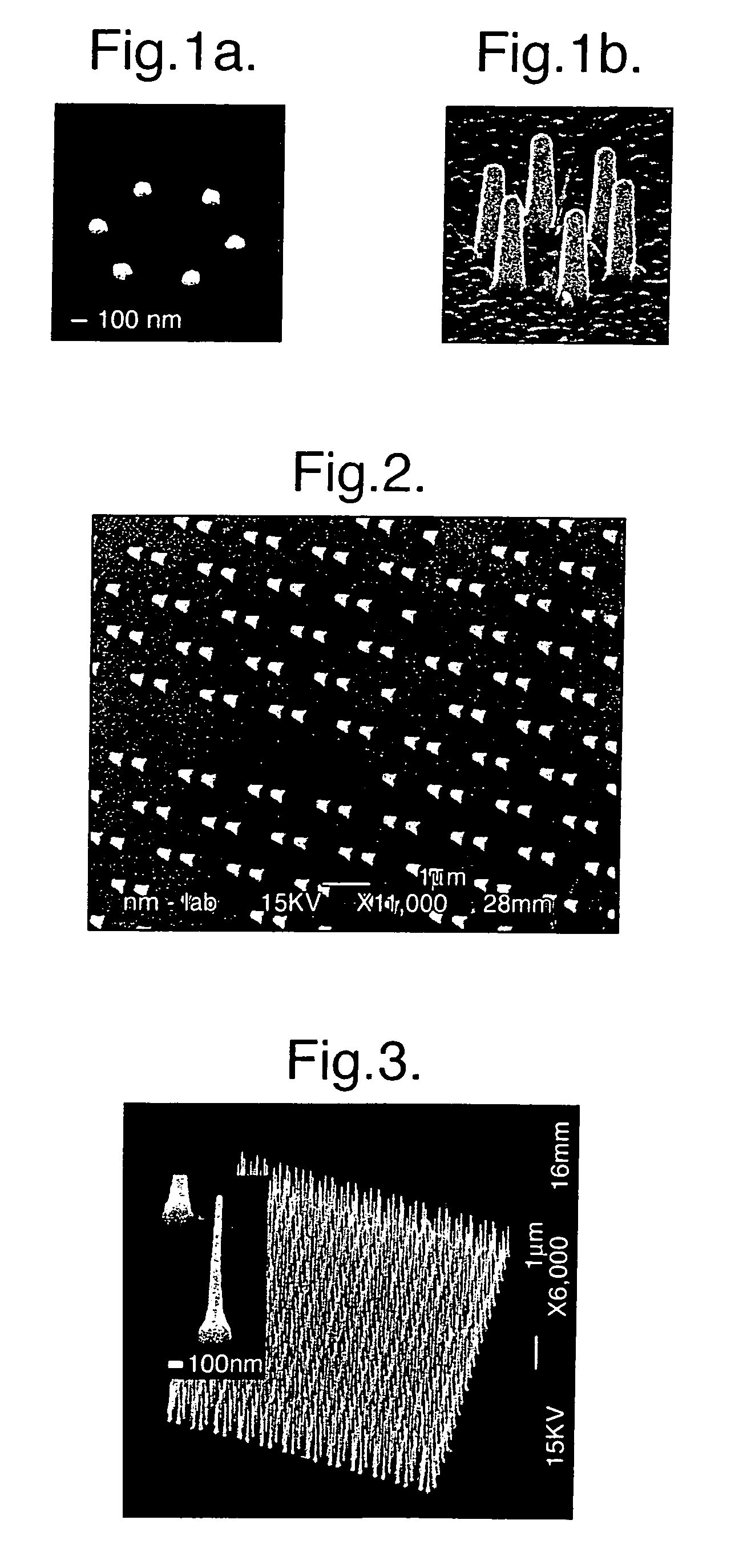
[0097]Samples were prepared from an n-type InP (111)B wafer. The (111)B substrate orientation was chosen since it is well known that the preferred wire growth direction is (111) B. The samples were cleaned on a spinner with acetone and isopropanol (IPA). They were then coated with poly(methylmethacrylate) (PMMA) photoresist and the disc pattern was transferred to the resist layer using a standard EBL technique. After development in methyl isobutyl ketone (MIBK) and rinsing in IPA, the samples were treated briefly with oxygen plasma to remove any resist residues from the exposed areas. After plasma treatment they were etched for 20 s in 4% hydrofluoric acid to remove surface oxide. The samples were then immediately transferred to a vacuum chamber where a gold film was deposited (thickness ranging from 17 to 45 nm and diameters of 125 nm) via thermal evaporation. The thickness was measured using a quartz crystal monitor. After metal lift-off by dissolution of the photoresist layer in ...
example 2
[0098]This example is based on nano-imprint lithography (NIL). NIL is in many respects capable of producing results comparable to those of electron beam lithography (EBL), but at a considerably lower cost and with a much higher throughput. NIL was used to pattern InP substrates with growth-catalyzing gold particles. Growth of vertically aligned InP nanowires then took place in a metal-organic vapor phase epitaxy (MOVPE) system via the vapor-liquid-solid (VLS) growth. The material of choice was InP, but the method is effective equally well with other III-V materials. The (111)B substrate orientation was used since the preferred growth direction of nanowires is B, and vertically aligned arrays were desired.
[0099]The stamp for the nano-imprint process was made on a one-inch Si wafer using EBL and dry etching. A bi-layer of resist was used comprising ZEP520A7 / PMMA950k that was exposed at 35 kV with a probe current of 20 pA. After resist development, 30 nm of Chromium was thermally evapo...
example 3
[0117]As shown in FIG. 8, a mask of silicon nitride, 27 nm thick, was formed on an InP substrate. Circular apertures were formed in the mask by a lithographic process. Gold catalytic particles were formed in the circular apertures within the mask. Nanowhiskers were grown form the gold catalytic particles. The nanowhiskers substantially filled the mask apertures, with a narrow gap between the nanowhisker and the edge of the mask aperture.
PUM
| Property | Measurement | Unit |
|---|---|---|
| thickness | aaaaa | aaaaa |
| size | aaaaa | aaaaa |
| diameter | aaaaa | aaaaa |
Abstract
Description
Claims
Application Information
 - R&D
- Intellectual Property
- Life Sciences
- Materials
- Tech Scout
- Unparalleled Data Quality
- Higher Quality Content
- 60% Fewer Hallucinations
Browse by: Latest US Patents, China's latest patents, Technical Efficacy Thesaurus, Application Domain, Technology Topic, Popular Technical Reports.
© 2025 PatSnap. All rights reserved.Legal|Privacy policy|Modern Slavery Act Transparency Statement|Sitemap|About US| Contact US: help@patsnap.com


