Method and apparatus for rapid thermal processing and bonding of materials using RF and microwaves

a technology of radio frequency and microwave, which is applied in the direction of manufacturing tools, induction current sources, electric/magnetic/electromagnetic heating, etc., can solve the problems of slow heating rate, mismatch of resonant frequencies between rf/microwave sources, and slow heating rate of conventional heating, so as to achieve fast microwave heating and poor microwave absorber

Active Publication Date: 2009-08-04
TIAN YONGLAI +1
View PDF7 Cites 7 Cited by
  • Summary
  • Abstract
  • Description
  • Claims
  • Application Information

AI Technical Summary

Benefits of technology

[0024]To overcome the limitations in the prior art described above, the present invention discloses a method and apparatus for rapid and selective heating of materials using variable frequency RF / microwave sources. The method and apparatus can provide ultra-high heating speed along with ultra-high heating temperatures for RTP of materials that other RTP techniques can not perform. It also will provide a new approach to meet the challenges of high interconnect density of integrate circuits and high bonding quality for mems applications.
[0025]The primary objective of the present invention is to disclose a RF / microwave apparatus which is capable of rapid and selective heating of materials to very high temperature. The heating rate depends on how efficiently the RF / microwave energy is coupled into the targeted materials. The RF / microwave apparatus of the present invention has a number of advantages which overcome the limitation of prior art in microwave heating techniques and significantly improves the efficiency of microwave coupling.
[0026]Another objective of the present invention is to teach a method for rapid thermal processing of semiconductors and materials using an RF / microwave apparatus. Experiments based on this method for rapid heating of SiC wafers and Arsenic (As) doped Si wafers have demonstrated that the RF / microwave apparatus of this invention has the capability of achieving ultra-high temperature of over 2000° C. and an ultra-fast heating rate of 2,000° C. / second.

Problems solved by technology

Conventional heating is slow because the heat is applied to the surface of an object.
There are three forms of interaction in general, namely: (1) materials with low complex dielectric constant are poor microwave absorbers and not good for microwave heating; (2) materials with high complex dielectric constant are strong microwave absorber and very good for microwave heating; and, (3) conductors such as metals reflects microwave so not good for microwave heating in general.
There are some technical barriers for further increasing the heating rate to well above 100° C. / sec level using cavity techniques used in prior art.
First the use of a fixed frequency source leads to a mismatch in resonant frequencies between the RF / microwave source and the loaded cavity when the frequency of the loaded cavity shifts with the temperature changes during a thermal process.
Second, the cavity is mechanically tuned so its response to coupling change is slow which results in a slow down of the heating rate.
There are other limitations of cavity coupling techniques in the prior art.
One of the significant problems is the arcing and the breakdown of plasma inside the cavity as the input RF / microwave power reaches a threshold level to breakdown the air.
The limitation of input power due to the arcing problem significantly limits the ability of using cavity techniques to achieve high heating rate and high heating temperature.
Another limitation of cavity techniques used in the prior art is that the size of the load must be smaller than the size of the cavity.
Since the dimension of a single mode cavity decreases with an increase of the operating frequency, the size of the cavity operating at high frequency may not be large enough when the size of load is big, e.g. an 8″ silicon wafer.
However, the use of induction heating in prior art is limited in low frequency levels, ranged from 50 Hz to less than 50 MHz.
None of the induction heating methods in the prior art has used RF and microwave frequency beyond 100 MHz.
Induction heating in not suitable in heating low conductive materials and insulators due to the lack of eddy current.3. Applications
By increasing the annealing temperature while simultaneously reducing the time, high percentage of electrical activation can be achieved and will lead to low sheet resistance.
None of conventional heating methods used in prior art can meet these requirements.
Limited by the slow heating rate, conventional furnace heating methods can only perform SiC annealing at temperatures below 1700° C. with annealing time longer than 5 minutes.
The relative low annealing temperature of below 1700° C. will result in ineffective recovery of crystal and low activation efficiency.
The halogen lamp based commercial RTP systems can only operate at below 1300° C. which makes them incapable for post implant annealing of SiC.
However, they will no longer meet the challenges in making ultra-shallow junctions associated with next generation CMOS in sub-65 nm regime or smaller where ultra-high heating rates well above 1000° C. / sec are required.
The large space occupied by the solder bumps becomes a limited fact for further shrinkage of the IC package.
Another problem with the soldering method is the high residual stress at the bonding interfaces caused by the large coefficient of thermal expansion (CTE) mismatch between the solder bump and the substrates.
The high residual stress may induce delamination and cracks in the package during the operation in thermal cycles.
Low temperature solder bonding can no longer meet these requirements because of its weak mechanical strength, low melting temperature and poor chemical resistance.
However, all these existing bonding techniques are global heating methods so entire mems are exposed to high temperatures for long processing times which may lead to some damages or changes of the microcircuits and microstructure which were already placed on the mems components.
Since the rapid thermal processes must be completed in a very short time, e.g. a few seconds or less, it is very hard to tune and to control the processes manually.
Meanwhile the bulk of silicon substrate remains cool because of the fast heating speed and short heating time.

Method used


Image

  • Method and apparatus for rapid thermal processing and bonding of materials using RF and microwaves
  • Method and apparatus for rapid thermal processing and bonding of materials using RF and microwaves
  • Method and apparatus for rapid thermal processing and bonding of materials using RF and microwaves

Examples


Embodiment Construction

RF / Micrwave Apparatus for Rapid and Selective Heating of Materials

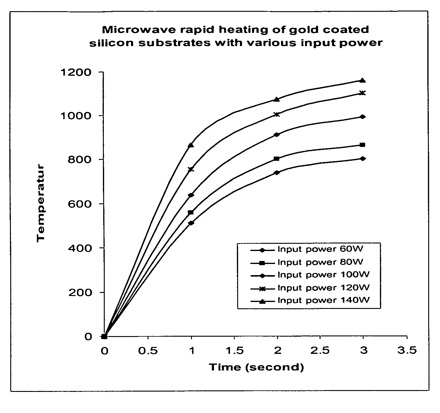
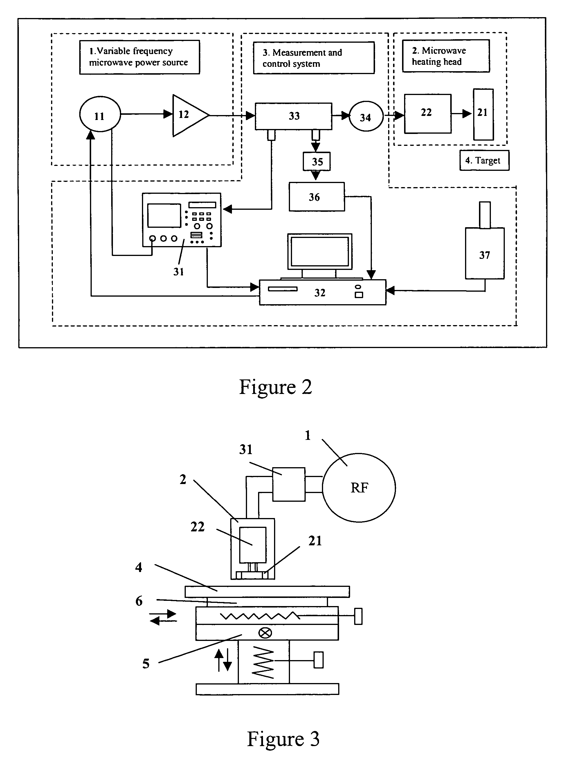
[0056]One objective of the present invention is to disclose a RF / microwave apparatus which is capable of rapid and selective heating of materials to very high temperature. FIG. 2 is a block diagram of the RF / microwave apparatus for rapid heating of materials according to the present invention. This RF / microwave apparatus can be divided in to three main parts: the variable frequency RF / microwave power source 1; the RF / microwave heating head 2; and, the measurement and control system 3. RF / microwave power is generated from a variable frequency power source 1, which is driven by solid state electronics and coupled into a target specimen 4 through a RF / microwave heating head 2. A measurement and control system 3, which is placed between 1 and 2, is used for tuning, monitoring and controlling of the RF / microwave thermal processes.

Solid State High Power RF / Microwave Sources

[0057]Still referring to FIG. 2, the variable frequ...


PUM

PropertyMeasurementUnit
driving frequencyaaaaaaaaaa
frequencyaaaaaaaaaa

Abstract

A method and apparatus for rapid and selective heating of materials using variable frequency RF and microwaves. The apparatus uses variable frequency solid state electronics as a microwave power source, a novel microwave heating head to couple microwave energy to the target materials and a match-up network to tune the frequency and impedance match between the microwave source and the load. An electronic and computer measurement and control system is employed to monitor and control the microwave heating process. The method teaches the use of inductive microwave coupling for thin conductive materials such as metal film and impurity doped silicon wafers. The method also teaches the use of capacitive microwave coupling for dielectric material such as glass and ceramics. The method further teaches the use of rapid and selective heating of heterostructure for bonding and sealing of mems and integrated circuits. The method and apparatus can provide ultra-high heating speed along with ultra-high heating temperatures for rapid thermal processing of semiconductors and other materials. It also allows the use of bonding materials with high melting temperature for strong bonding and sealing of mems and IC devices. The apparatus further provides for high interconnection density of integrated circuits as connections are made without the use of solder bumps.

Description

CROSS REFERENCE TO RELATED APPLICATIONS[0001]This application claims the benefit of U.S. Provisional Application No. 60 / 627,472, filed Nov. 15, 2004.BACKGROUND[0002]1. Field of Invention[0003]The present invention relates to rapid thermal processing and bonding of materials using radio frequencies (RF) and microwaves, and more specifically to a method and apparatus for rapid heating of materials using solid state variable frequency RF / microwave sources. The invention further relates to a method for rapid thermal processing of semiconductors and materials using the present RF / microwave apparatus. The present invention also relates to a method of selectively heating portions of materials using the RF / microwave apparatus of the invention, and more specifically to the bonding and sealing of microelectro-mechanical systems (mems) and integrated circuits (IC / microchips) using the present method of RF / microwave rapid and selective heating.[0004]2. Related ArtAdvantages of Rapid RF / Microwav...

Claims


Application Information

Patent Timeline
Patent Type & Authority Patents(United States)
IPC IPC(8): H05B6/08H05B6/04
CPCB23K13/01H01L21/50H05B6/806H01L24/75H05B6/68H01L2924/1461H01L2924/10253H01L24/81H01L2224/13144H01L2224/16H01L2224/75H01L2224/7525H01L2224/759H01L2224/81193H01L2224/8122H01L2224/81222H01L2224/81801H01L2224/81894H01L2924/01029H01L2924/01047H01L2924/01078H01L2924/01079H01L2924/01082H01L2924/01322H01L2924/09701H01L2924/14H01L2924/19041H01L2924/30105H01L2924/30107H01L2924/3011H01L2924/01005H01L2924/01006H01L2924/01024H01L2924/01033H01L2924/0105H01L2924/01074H01L2924/01076H01L2924/014H01L2924/00H01L2224/05568H01L2224/05573H01L2224/05644H01L2224/75266H01L2224/83234H01L2924/00014
Inventor TIAN, YONGLAITIAN, MARK Y.
Owner TIAN YONGLAI
Why Eureka
Try Eureka