
Wiring board with semiconductor component

a semiconductor and wiring board technology, applied in the field of electrical devices, can solve the problems of increasing the occurrence of disconnection failures, increasing the frequency of cracks to the solder joint portion, and prone to short circuits between adjacent joint portions, so as to achieve high melting point, prevent cracks, and high melting point

Inactive Publication Date: 2009-02-10
NGK SPARK PLUG CO LTD
View PDF4 Cites 23 Cited by
  • Summary
  • Abstract
  • Description
  • Claims
  • Application Information

AI Technical Summary

Benefits of technology

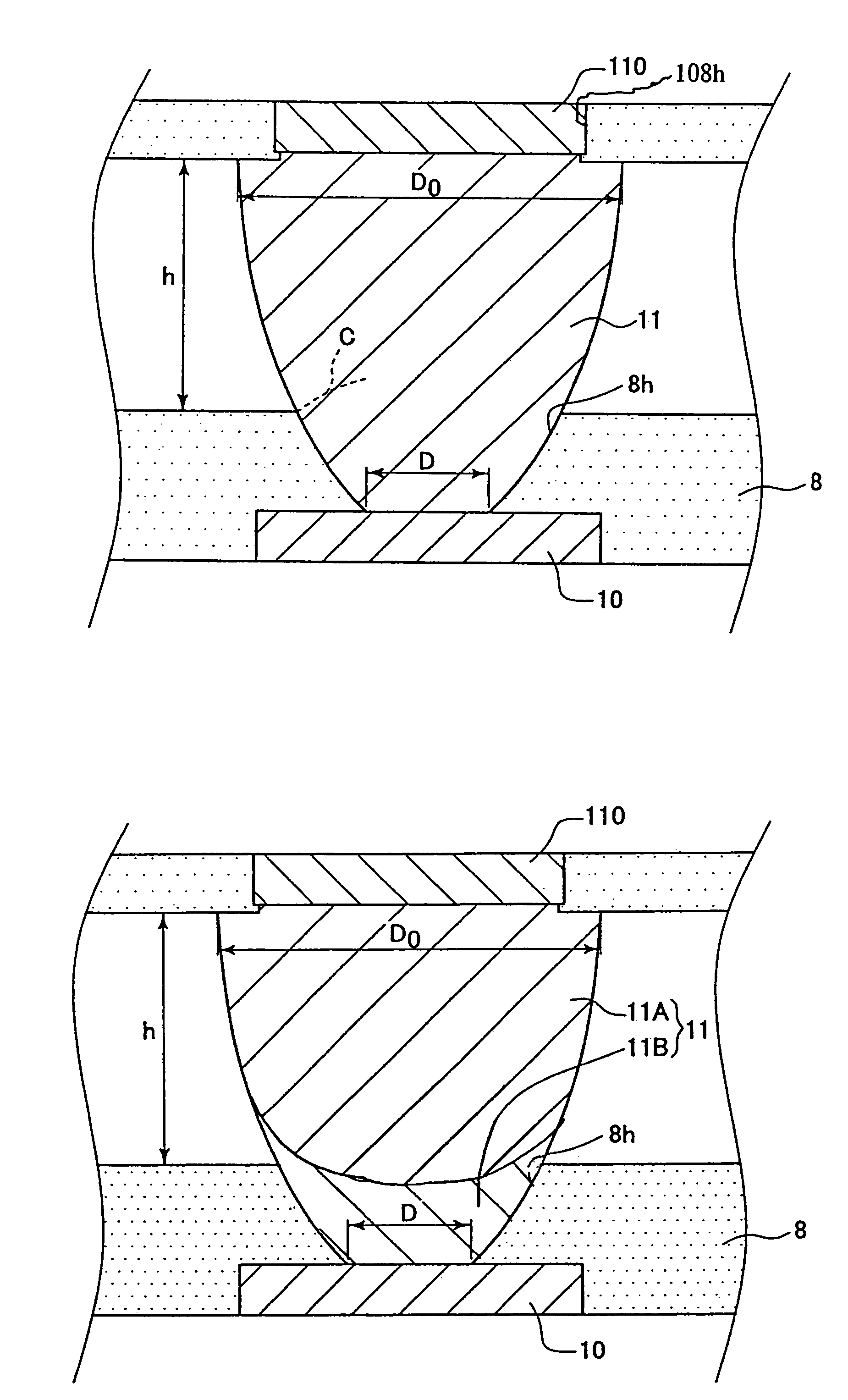
[0013]Effect of the present invention is particularly demonstrated when the solder joint portion is formed from a combination of a plurality of solder portions each made of a different composition. That is, discontinuous interface of metallographic structure, especially cracks due to thermal stress, is likely to occur in a boundary between solders each made of a different composition. However, the present invention drastically enables the prevention of cracks, even though the discontinuous interface is generated. Specifically, when the solder joint portion formed from a plurality of solders comprises (a) a first solder portion contacting the terminal at the board side and (b) a second solder portion contacting the first solder portion and the terminal at the component side, the second solder portion having a higher melting point than that of the first solder portion, the discontinuous interface of metallographic structure is likely to occur between the second solder portion at the component side having a high melting point and the first solder portion at the board side having a low melting point. Therefore, the application of the present invention, specifically, demonstrates the effectiveness.

Problems solved by technology

Also, it is unlikely that a frequency of crack occurrence to the solder joint portion may be especially high due to only a scale factor.
However, in reality, the narrower the clearance between the terminals becomes, the greater the occurrence of disconnection failures caused by cracks.
That is, in the terminal array at the board side positioned downward during reflow, the lower part of the solder joint portion spreads due to influence of melting solder flow, thereby a short circuit generated between adjacent joint portions tends to occur.

Method used


Image

  • Wiring board with semiconductor component
  • Wiring board with semiconductor component
  • Wiring board with semiconductor component

Examples


Embodiment Construction

[0021]Hereinafter, preferred embodiments of the present invention are explained with reference to the drawings.

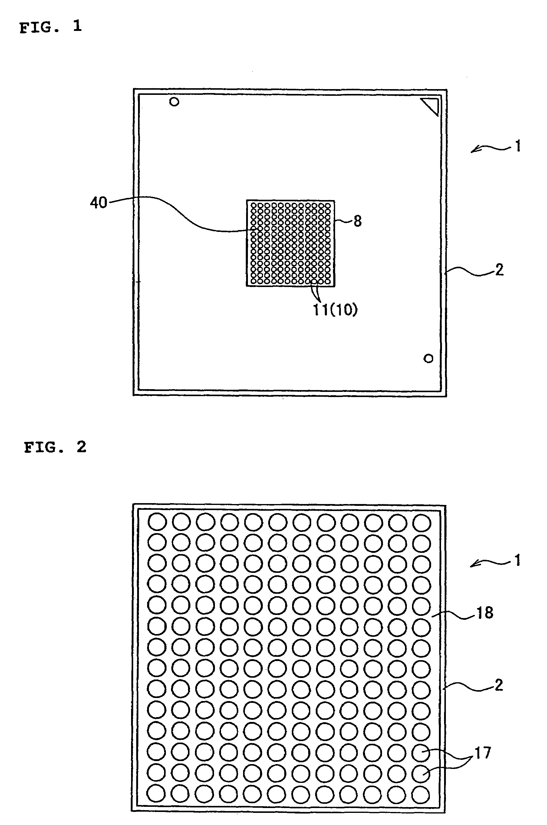
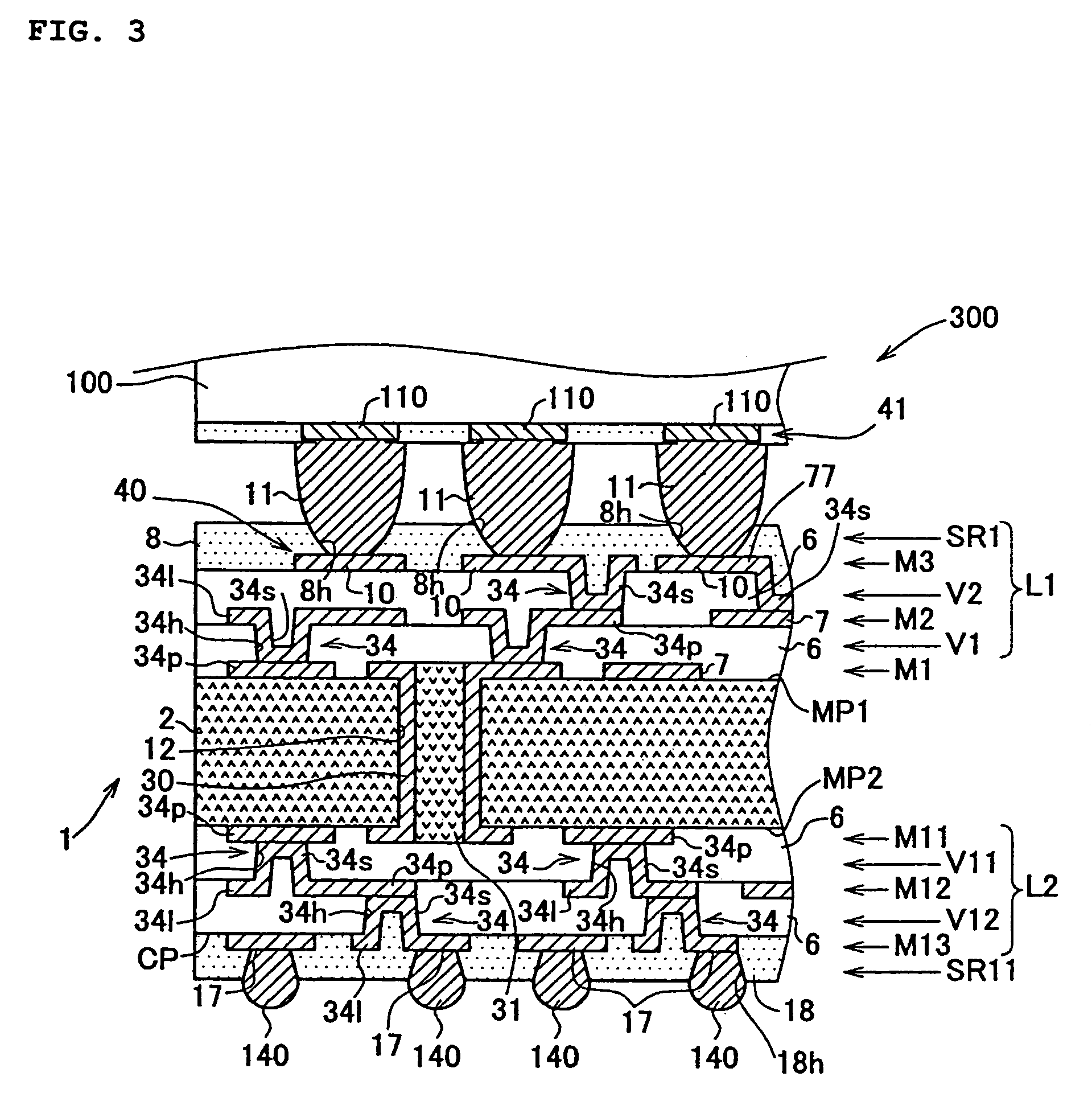
[0022]FIG. 3 shows a frame format of a cross sectional structure of a wiring board 300 with a semiconductor component according to an embodiment of the present invention. First, a wiring board 1 comprises a wiring laminated portion L1 including dielectric layers V1, V2 comprised of a polymer material and conductor layers M1, M2, M3, wherein the dielectric layers V1, V2 and the conductor layers M1, M2 are alternately laminated so that the dielectric layer V2 may form a first main surface of the wiring laminated portion L1. On the first main surface of the wiring laminated portion L1 formed of the dielectric layer V2, a plurality of metal terminal pads (hereinafter referred to as first pads at the board side or simply first pads) 10 are disposed in a lattice pattern (or a zigzag pattern) to form a pad array at a board side 40, as shown in FIG. 1.

[0023]As shown in FIG. 3, on t...


PUM


Abstract

An electronic device comprised of a wiring board with a semiconductor component. The device is unlikely to have any defects, such as cracks to a solder joint portion during a reflow process of a flip-chip connection. The semiconductor component is flip-chip bonded at a pad array at a component side thereof to a pad array at a board side by way of an individual solder joint portion. In a solder resist layer at a semiconductor component side and a solder resist layer at a board side, D / D0 is prepared to be in a range of 0.70 to 0.99, where D is a bottom inner diameter of an opening at the board side and D0 is a bottom inner diameter of an opening at the component side.

Description

FIELD OF THE INVENTION[0001]The present invention relates to an electronic device comprised of a wiring board with a semiconductor component.BACKGROUND OF THE INVENTION[0002]Among wiring boards for use in connecting a semiconductor component, such as an integrated circuit (IC) or a large-scale integration (LSI), the so-called organic package substrate comprises a wiring laminated portion and a pad array. The wiring laminated portion includes a plurality of dielectric layers comprised of a polymeric material and a plurality of conductor layers. The plurality of dielectric layers and the plurality of conductor layers are alternately laminated so that the dielectric layer may form a first main surface of the wiring laminated portion. The pad array formed at the board side is comprised of a plurality of metal terminal pads formed on the first main surface, which is formed of said dielectric layer, of said wiring laminated portion. A terminal array is formed at a component side on a seco...

Claims


Application Information

Patent Timeline
Patent Type & Authority Patents(United States)
IPC IPC(8): H05K1/16
CPCH01L23/49816H05K3/3436H05K3/3452H05K3/3463H05K2201/09427H05K2201/099H05K2201/10992H05K2203/0465H05K2203/0594H01L2224/81191H01L2924/01322H01L2924/00Y02P70/50
Inventor SAIKI, HAJIMEIBA, MASAHIRO
Owner NGK SPARK PLUG CO LTD
Learn More