Amplifying circuit
a circuit and amplifier technology, applied in the field of electric power consumption reduction techniques, can solve the problems of large circuit construction, increased self electric power consumption of the charge pump itself, etc., and achieve the effect of reducing electric power consumption and simple circuit construction
- Summary
- Abstract
- Description
- Claims
- Application Information
AI Technical Summary
Benefits of technology
Problems solved by technology
Method used
Image


Examples
embodiment 1
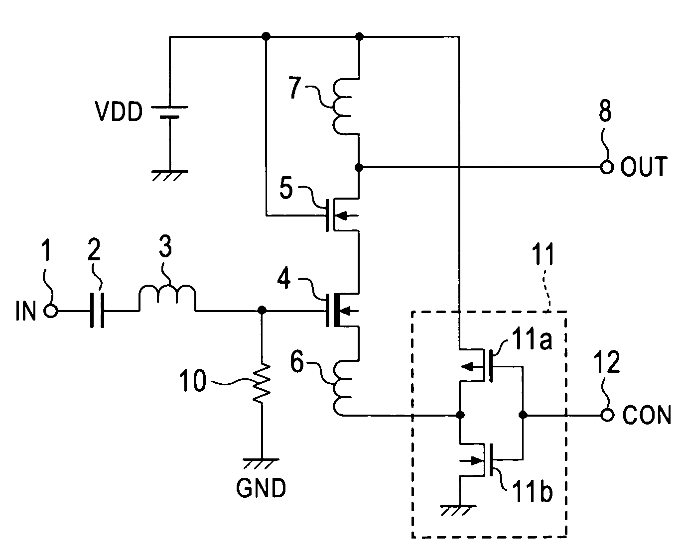
[0031]FIG. 2 is a constructional view of an LNA for a high frequency showing the present invention. Reference numerals common to those in FIG. 1 are designated in elements common to those within FIG. 1.
[0032]This LNA is assembled into a high frequency LSI of one chip manufactured by directly forming an active element such as a transistor and a diode and a passive element such as a resistor, an inductor, a capacitor, etc. on a SOI substrate or a SOS substrate forming a silicon thin film on the surfaces of a silicon substrate and an insulating substrate of quartz and sapphire by a CMOS process technique.
[0033]Similar to the LNA of FIG. 1, this LNA has a capacitor 2 and an inductor 3 constituting a filter circuit for interrupting a direct electric current from an input signal IN given to a node 1 and fetching a signal of a predetermined frequency area. A cascode-connected amplifying section is connected to the output side of this inductor 3. The amplifying section has a DMOS 4 of an in...
embodiment 2
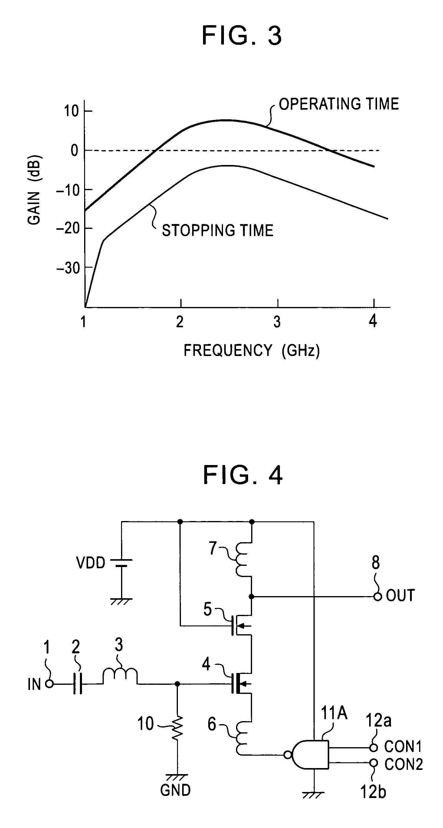
[0044]FIG. 4 is a constructional view of an LNA for a high frequency showing the present invention. Reference numerals common to those in FIG. 1 are designated in elements common to those within FIG. 1.
[0045]In this LNA, a NAND gate 11A of two inputs is arranged instead of the inverter 11 within FIG. 1. The NAND gate 11A inverts and outputs a logical product of control signals CON, CON2 given to nodes 12a, 12b. The other constructions are similar to those of FIG. 1.
[0046]The operation of this LNA is similar to the operation of the LNA of FIG. 1 except that the operating state is controlled by combining the control signals CON, CON2. Accordingly, this LNA has advantages similar to those of the LNA of FIG. 1. Other logical gates can be used instead of the NAND gate 11A.
embodiment 3
[0047]FIG. 5 is a constructional view of an LNA for a high frequency showing the present invention. Reference numerals common to those in FIG. 1 are designated in elements common to those within FIG. 1.
[0048]In this LNA, an amplifying section using a DMOS 14 is connected to the node 8 in the LNA of FIG. 1 through a capacitor 13. Namely, one end of the capacitor 13 is connected to the node 8, and the other end is connected to the gate of the DMOS 14. A grounding voltage GND is applied to the gate of the DMOS 14 through a resistor 15, and the source of the DMOS 14 is connected to the output side of the inverter 11 through an inductor 16. Further, an electric power source voltage VDD is applied to the drain of the DMOS 14 through a load impedance 17, and this drain of the DMOS 14 is connected to a node 18. An output signal OUT is outputted from this node 18. The other constructions are similar to those of FIG. 1.
[0049]The operation of this amplifying circuit will next be explained.
[005...
PUM
 Abstract
Description
Claims
Application Information
 - R&D
- Intellectual Property
- Life Sciences
- Materials
- Tech Scout
- Unparalleled Data Quality
- Higher Quality Content
- 60% Fewer Hallucinations
Browse by: Latest US Patents, China's latest patents, Technical Efficacy Thesaurus, Application Domain, Technology Topic, Popular Technical Reports.
© 2025 PatSnap. All rights reserved.Legal|Privacy policy|Modern Slavery Act Transparency Statement|Sitemap|About US| Contact US: help@patsnap.com