Resist pattern thickening material, process for forming resist pattern, and process for manufacturing semiconductor device

a technology of resist pattern and thickening material, which is applied in the direction of photosensitive materials, instruments, photomechanical equipment, etc., can solve the problems of difficult development of new resist materials suitable for exposure using short wavelength light sources, high cost, etc., and achieve the effect of reducing cost and facilitating production

Active Publication Date: 2008-04-29
FUJITSU LTD
View PDF35 Cites 0 Cited by
  • Summary
  • Abstract
  • Description
  • Claims
  • Application Information

AI Technical Summary

Benefits of technology

[0007]An object of the present invention is to provide a process for forming a resist pattern which, when patterning a resist pattern to be thickened, can utilize, as is, light sources (such as ArF excimer laser light and the like) of existing exposure devices, and which has excellent mass productivity, and which can finely, uniformly, and stably form a space pattern having reduced surface roughness, exceeding the exposure limits of such light sources, regardless of the material and the size of the resist pattern to be thickened.
[0008]Another object of the present invention is to provide a resist pattern thickening material which, when applied on a resist pattern to be thickened, can efficiently, uniformly, and stably thicken the resist pattern to be thickened so that a thickened resist pattern has reduced surface roughness, regardless of the material and the size of the resist pattern to be thickened, and which is suitable for forming a fine space pattern, exceeding the exposure limits of light sources of existing exposure devices.
[0009]Yet another object of the present invention is to provide a process for manufacturing a semiconductor device which, by using a space pattern which has been formed to be fine and uniform using the resist pattern, can form a fine pattern on an underlying layer which is an oxide film or the like, and which can efficiently mass produce high-performance semiconductor devices having fine wiring and the like.
[0010]The resist pattern thickening material of the present invention comprises a resin, a crosslinking agent, and a nitrogen-containing compound. When the resist pattern thickening material is applied onto a resist pattern to be thickened, among the applied resist pattern thickened material, the portions thereof which are in a vicinity of the interface with the resist pattern to be thickened seep into the resist pattern to be thickened and crosslink with the material of the resist pattern to be thickened. At this time, because the affinity of the resist pattern thickening material and the resist pattern to be thickened is good, a surface layer, in which the resist pattern thickening material and the resist pattern to be thickened have become integral, is formed efficiently on the surface with the resist pattern to be thickened being the inner layer. (The resist pattern to be thickened is efficiently thickened by the resist pattern thickening material.) The resist pattern formed in this way (which will be called “thickened resist pattern” upon occasion hereinafter) is uniformly thickened by the resist pattern thickening material. Thus, a space pattern formed by the resist pattern exceeds exposure limits and has a more fine structure. Because the resist pattern thickening material of the present invention contains a nitrogen-containing compound, a good, uniform thickening effect is exhibited regardless of the type of the material, the size or the like of the resist pattern to be thickened, and there is little dependence on the material and the size of the resist pattern to be thickened. Further, even if free acids are generated while the resist pattern thickening material is being stored, the free acids are neutralized by the nitrogen-containing compound. Thus, the resist pattern thickening material is always maintained at a constant pH, and the storage stability thereof is excellent. The pH of the resist pattern thickening material does not decrease during storage, or due to the temperature conditions or the like. Therefore, stable thickening is always possible without being affected by the temperature conditions at the time of thickening, the storage conditions, or the like. The process margin can be ensured, and the roughness of the surface of the resist pattern can be decreased. Furthermore, the stable pH prevents the applied resist pattern thickening material from crosslinking throughout its entire portion.
[0012]A process for forming a semiconductor device of the present invention comprises: applying the resist pattern thickening material of the present invention after forming a resist pattern to be thickened on an underlying layer so as to cover a surface of the resist pattern to be thickened, thereby thickening the resist pattern to be thickened and forming a resist pattern; and patterning the underlying layer by etching using the resist pattern. In the process for forming a semiconductor device of the present invention, after a resist pattern to be thickened has been formed on the underlying layer, the resist pattern thickening material is applied on the resist pattern to be thickened. Among the applied resist pattern thickening material, the portions thereof which are in a vicinity of the interface with the resist pattern to be thickened seep into the resist pattern to be thickened and crosslink with the material of the resist pattern to be thickened. Thus, a surface layer, in which the resist pattern thickening material and the resist pattern to be thickened have become integral, is formed on the surface with the resist pattern to be thickened being the inner layer. The resist pattern formed in this way is uniformly thickened by the resist pattern thickening material. Thus, the space pattern formed by the resist pattern exceeds exposure limits and has a finer structure. Then, the underlying layer is patterned by etching by using this pattern as a mask. Thus, a high-quality, high-performance semiconductor device having an extremely fine pattern can be manufactured efficiently.

Problems solved by technology

However, in order to make a light source of an exposure device be a short wavelength, it is necessary to update the exposure device, which results in very high costs.
Further, the development of new resist materials which is suitable to exposure using short wavelength light sources is not easy.
Accordingly, the current situation is that there has not yet been provided a technique which can use light as the light source of an exposure device at the time of patterning, and which can form with high detail a uniform and fine space pattern.

Method used


Image

  • Resist pattern thickening material, process for forming resist pattern, and process for manufacturing semiconductor device
  • Resist pattern thickening material, process for forming resist pattern, and process for manufacturing semiconductor device
  • Resist pattern thickening material, process for forming resist pattern, and process for manufacturing semiconductor device

Examples


example 1

Preparation of Resist Pattern Thickening Material

[0149]Resist pattern thickening materials A through F of the present invention having the compositions shown in Table 1 were prepared. Note that, in Table 1, the unit of the values in parentheses is parts by mass. In the “resin” column, “KW-3” is a polyvinyl acetal resin (manufactured by Sekisui Chemical Co., Ltd.). In the “crosslinking agent” column, “uril” is tetramethoxymethylglycol uril, and “urea” is N,N′-dimethoxymethyldimethoxyethylene urea. In the “surfactant” column, “TN-80” is a non-ionic surfactant (a polyoxyethylene monoalkylether surfactant manufactured by Asahi Denka Co., Ltd.). Further, a mixed liquid of pure water (deionized water) and isopropyl alcohol (whose mass ratio was pure water (deionized water):isopropyl alcohol=82.6:0.4) was used as the other main solvent component other than the resin, the crosslinking agent, and the nitrogen-containing compound.

[0150]

TABLE 1organicthickeningcross-linkingnitrogen-containings...

example 2

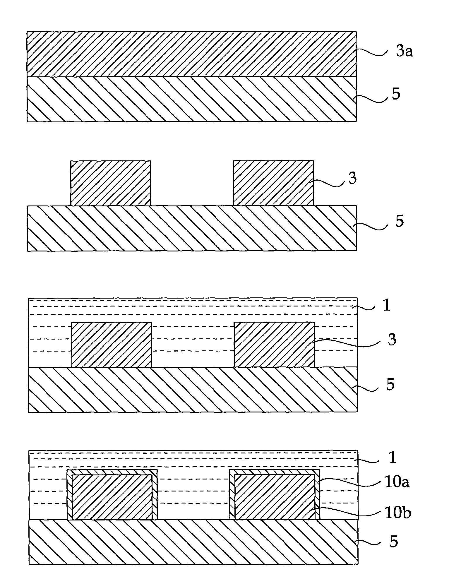
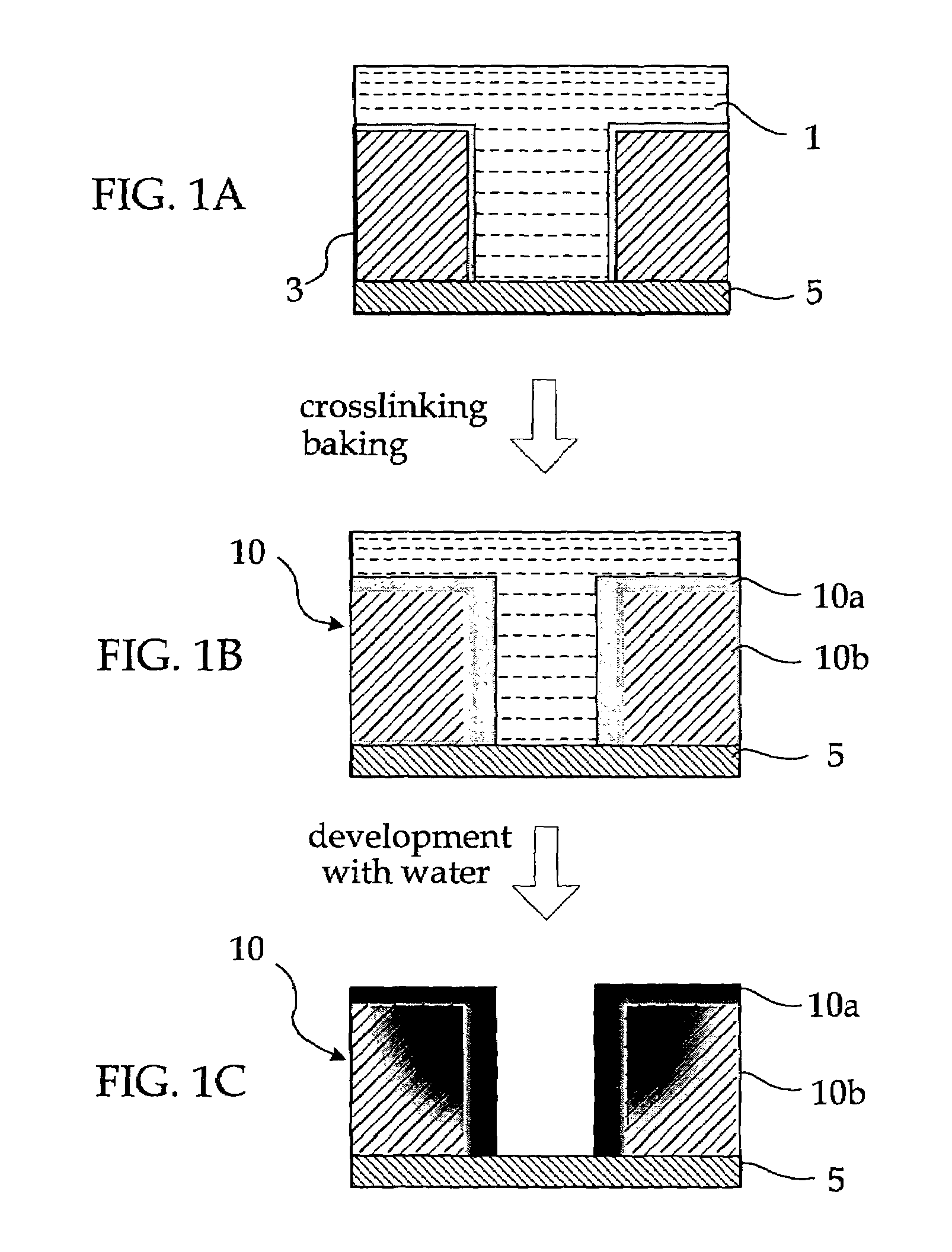
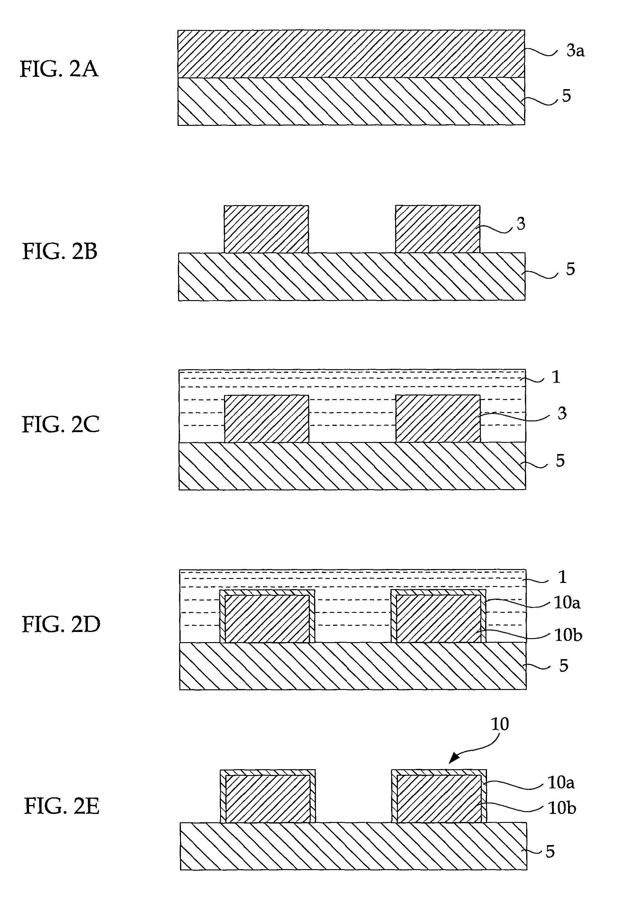
[0161]As shown in FIG. 3A, an interlayer insulating film 12 was formed on a silicon substrate 11. As shown in FIG. 3B, a titanium film 13 was formed by a sputtering method on the interlayer insulating film 12. Next, as shown in FIG. 3C, a resist pattern 14 was formed. By using the resist pattern 14 as a mask, the titanium film 13 was patterned by reactive ion etching so that openings 15a were formed. Subsequently, as shown in FIG. 3D, the resist pattern 14 was removed by reactive ion etching, and openings 15b were formed in the interlayer insulating film 12 by using the titanium film 13 as a mask.

[0162]Next, the titanium film 13 was removed by wet processing, and as shown in FIG. 4E, a TiN film 16 was formed on the interlayer insulating film 12 by a sputtering method. Subsequently, a Cu film 17 was grown by an electrolytic plating method on the TiN film 16. Next, as shown in FIG. 4F, leveling was carried out by CMP so that the barrier metal and the Cu film (first metal film) remaine...

example 3

Flash Memory and Process for Manufacturing Thereof

[0166]Example 3 is an example of the semiconductor device and process for manufacturing thereof of the present invention using the resist pattern thickening material of the present invention. Note that, in Example 3, resist films 26, 27, 29, 32 and 34 which will be described hereinafter are resist films which have been thickened by the same process as in Examples 1 and 2 by using the resist pattern thickening material of the present invention.

[0167]FIGS. 6A and 6B are top views (plan views) of a FLASH EPROM which is called a FLOTOX type or an ETOX type. Note that FIGS. 7A through 7C, FIGS. 8D through 8F, and FIGS. 9G through 9I are cross-sectional schematic views for explaining an example of a process for manufacturing the FLASH EPROM. In FIGS. 7A through 9I, the illustrations at the left sides are the memory cell portion (a first element region), and are schematic diagrams of the cross-section (the A direction cross-section) of the ...


PUM

PropertyMeasurementUnit
Sizeaaaaaaaaaa
Sizeaaaaaaaaaa
Sizeaaaaaaaaaa

Abstract

The present invention provides a resist pattern thickening material which can thicken a resist pattern to be thickened regardless of a material or a size thereof so as to form a fine space pattern, exceeding an exposure limit of exposure light. The resist pattern thickening material comprises: a resin; a crosslinking agent; and a nitrogen-containing compound. In a process for forming a resist pattern of the present invention, the resist pattern thickening material is applied on a surface of a resist pattern to be thickened, thereby forming a resist pattern. A process for manufacturing a semiconductor device of the present invention includes: applying the thickening material on a surface of a resist pattern to be thickened which is formed on an underlying layer, so as to thicken the resist pattern to be thickened and form a resist pattern; and patterning the underlying layer by etching using the resist pattern.

Description

CROSS-REFERENCE TO RELATED APPLICATIONS[0001]This application is based upon and claims the benefit of priority from the prior Japanese Patent Application No. 2002-240082, filed on Aug. 21, 2002, the entire contents of which are incorporated herein by reference.BACKGROUND OF THE INVENTION[0002]1. Field of the Invention[0003]The present invention relates to a resist pattern thickening material, which is applied onto a resist pattern to be thickened and thickens the resist pattern to be thickened, and which can form a fine space pattern by exceeding exposure limits of light sources of existing exposure devices (“space pattern” is hereby defined as a hole, trench, recess, or any other empty space that is formed by a developed (removed) resist). The present invention also relates to a process for forming a resist pattern and a process for manufacturing a semiconductor device, which use the resist pattern thickening material.[0004]2. Description of the Related Art[0005]Semiconductor integ...

Claims


Application Information

Patent Timeline
IPC IPC(8): G03C1/73G03F7/038G03F7/30G03F7/36G03F7/38G03F7/004G03F7/00G03F7/40G11B5/17G11B5/31H01L21/027H01L21/3065H01L21/311H01L21/3213H01L21/8247H01L27/105
CPCG03F7/0035G03F7/40H01L21/31144H01L21/32139H01L27/105H01L27/11526H01L27/11543H01L21/0273G11B5/17G11B5/313G11B5/3163Y10S430/11H10B41/48H10B41/40G03F7/004
Inventor KOZAWA, MIWANOZAKI, KOJINAMIKI, TAKAHISAKON, JUNICHI
Owner FUJITSU LTD
Why Eureka
Try Eureka