Wafer machining adhesive tape, and its manufacturing method and using method

a technology of wafer machining and adhesive tape, which is applied in the direction of film/foil adhesives, synthetic resin layered products, transportation and packaging, etc., can solve the problems of chipping or fragmentation and cracking, chip failure, and circuitry corrosion of the chip

Inactive Publication Date: 2008-04-15
MITSUI CHEM INC
View PDF20 Cites 165 Cited by
  • Summary
  • Abstract
  • Description
  • Claims
  • Application Information

AI Technical Summary

Benefits of technology

[0015]The present inventors, as a fruit of their strenuous research efforts to resolve the aforementioned problems, have found that internal stress and vibrations which are generated in the course of the wafer processing may be mitigated extensively by fixing in place the wafer by means of attaching the wafer to the adhesive tape with such adhesive layer interposed in between that has a specific modulus within a certain wafer processing temperature range, or furthermore a specific tan δ within said temperature range. And, the present inventors have arrived at the present invention, having found the possibility of lessening and reducing the sizes of nick and crack in the wafer to the level never achieved before with the conventional wafer processing adhesive tape.
[0016]Accordingly it is an object of the present invention to provide such wafer processing adhesive tape that is capable of decreasing the sizes of nick and crack and also oppressing the development thereof in the course of cutting the wafer into chips. It is a further object of the present invention to provide such wafer processing adhesive tape that is capable of mitigating contamination of the chip without utilizing any special equipment, possesses long-term storage stability and is constructed of such raw materials that would not create much ecological burden.
[0017]It is another object of the present invention to provide such method for manufacturing wafer processing adhesive tape that gives stable product qualities and is capable of minimizing quantities of by-produced harmful materials and / or wastes or energies consumed in the production line, which conditions serving to make such manufacturing process to be adapt to the environments.
[0018]It is another object of the present invention to provide a method for using the wafer processing adhesive tape to the extent that its properties can be fully exploited.
[0019]Namely, the present invention relates to a wafer processing adhesive tape having an adhesive layer on one side of a substrate layer, which enables a silicon wafer of a 6-inch diameter adhered to said adhesive layer and ground on its backside to a 400 μm thickness to achieve production of chips having a maximum length of chipping or fragmentation (nicks) or crack of 30 μm or less by a ratio of 90% or higher as compared with a total number of chips obtained from a silicon wafer, when the silicon wafer is cut into 3 mm square size by full cutting using a dicer at a temperature of 15 to 35° C. and under conditions of a dicing speed of 70 mm / min. and cutting water maintained at a temperature of 20° C.

Problems solved by technology

The use of either type poses the problem of chipping or fragmentation and crack, which develop during the operation of cutting the wafer into chips.
Such sawdust could cause corrosion of the circuitry in the chip or deterioration of the bond between the chip and the resin molding so far as it causes failure of chips.
Moreover, the wafer processing adhesive tape having an adhesive layer of the pressure sensitive type, or the ultraviolet irradiation curing type or the electron beam curing type poses such problem that its service life is short because of its inferior fabrication phase stability and long-term storage stability, which problem necessitating well-managed workshop environments, transportation and storage conditions.
With the wafer processing adhesive tapes of these kinds, once deterioration of the adhesive layer progressed due to some unstable factors in the manufacturing conditions or storage conditions, there used to take place production of massive quantities of off-quality chips due to qualities of the wafer processing adhesive tape.
Said method charges a great ecological burden on the environment due to the use of organic solvent when applying the preparation and consumption of much energy for evaporating the solvent.
Worse still, it ends up with a higher cost.
This method is, however, accompanied by very low productivity, so that it is not employed conventionally in the semiconductor industry for processing those wafers on which circuit patters have been already formed except when brittle wafers are processed or the wafer surface is required to be finished with high precision.
Nevertheless, it does not clearly teach the sizes of such nick and crack that would conceivably develop in the chip during the grinding operation.
Obviously, there has been available no such wafer processing adhesive tape that would be capable of minimizing the sizes of nick and crack which develop during the wafer processing to a level comparable to the one achieved according to the wax-fixing method.

Method used


Image

  • Wafer machining adhesive tape, and its manufacturing method and using method
  • Wafer machining adhesive tape, and its manufacturing method and using method
  • Wafer machining adhesive tape, and its manufacturing method and using method

Examples


example 1

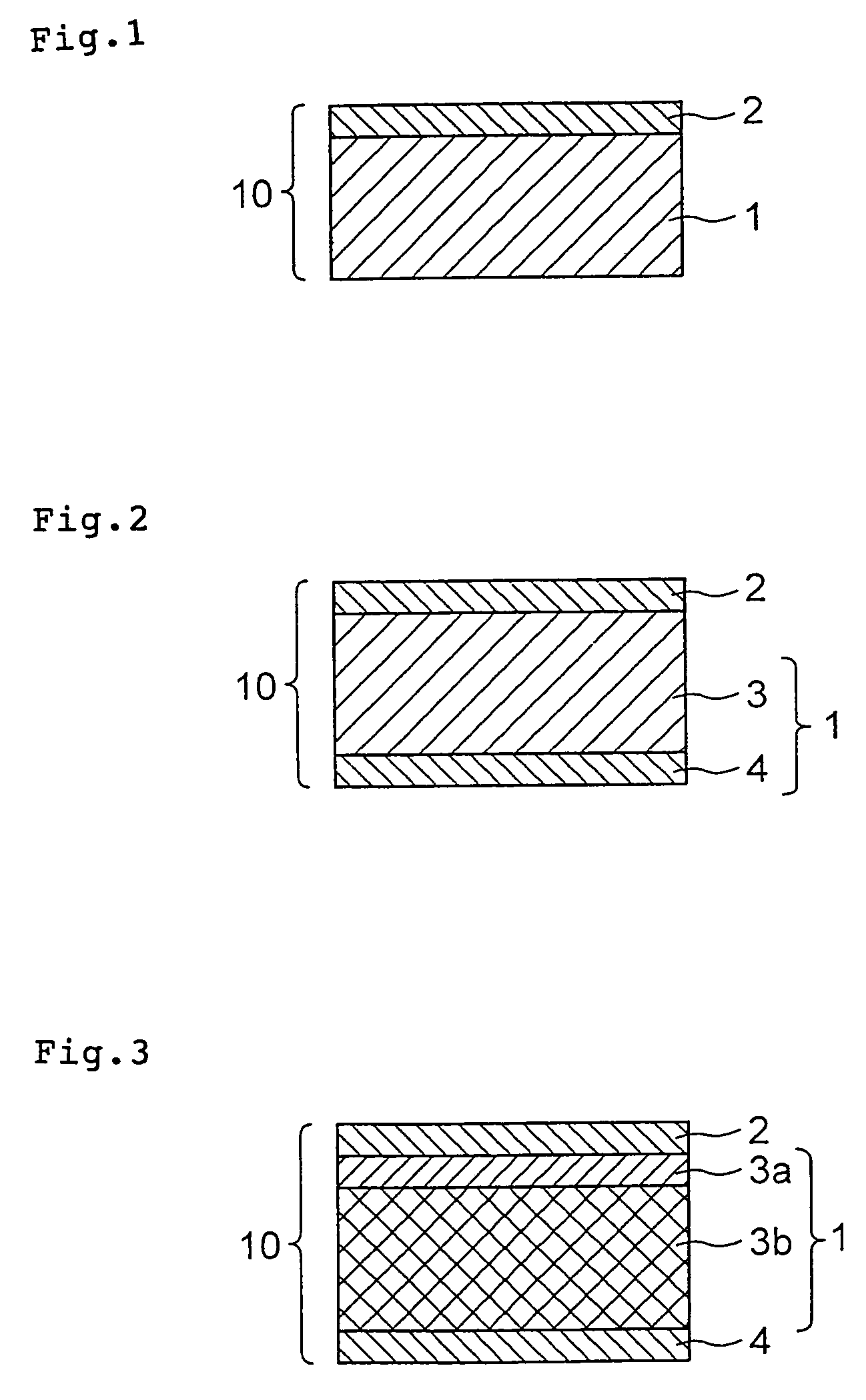
[0165]The following materials were used as the raw materials for the respective layers constituting the adhesive tape 10. As the components to constitute the substrate layer 1, 80 parts by weight of propylene-ethylene-1-butene random copolymer (r-PP) (consisting of 5 mol. % of ethylene, 5 mol. % of 1-butene) and 20 parts by weight of styrene-ethylene-butylene-styrene block copolymer (SEBS) (Taftec™ H1052 manufactured by Asahi Chemical Industry Co.) were used. As the components to constitute the adhesive layer 2, 100 parts by weight of propylene-1-butene-4-methyl-1-pentene copolymer (PB(4-MP)) (consisting of 50 mol. % of propylene, 20 mol. % of 1-butene, and 30 mol. % of 4-methyl-1-pentene) was used. FIG. 12 shows the storage modulus G′, loss modulus G″, and tan δ of the adhesive layer which were measured in accordance with the aforesaid procedure for measuring said viscoelasticity.

[0166]The melt flow rate of each layer was adjusted to 15 g / 10 min. for the adhesive layer and 15 g / 10 ...

example 2

[0177]For the raw materials for the respective layers constituting the adhesive tape 10, 80 parts by weight of the same r-PP as used in Example 1 and 20 parts by weight of hydrogenated styrene-isoprene-styrene block copolymer (SEPS) (Septon™ 2063 manufactured by Kuraray Co. Ltd.) were used as the components of the substrate layer 1. As the components of the adhesive layer 2, 95 parts by weight of the same PB(4-MP) as used in Example 1 and 5 parts by weight of ethylene-α-olefin co-oligomer (LEO) (Lucant™ HC-20 manufactured by Mitsui Chemicals, Inc.) were used. The test results covering the viscoelasticity of the adhesive layer are shown in Table 3 for the three different temperature levels of 15° C., 25° C. and 35° C.

[0178]Under the conditions shown in Table 1, an adhesive tape was formed in a same manner as employed in Example 1. After providing a release tape (Tohcello Separator™ SP T-18, thickness: 37 μm manufactured by Tohcello Co.) on the adhesive layer, the adhesive tape was sl...

example 3

[0180]For the raw materials for the respective layers constituting the adhesive tape 10, low-density poly-ethylene (LDPE) (density: 0.92 g / cm3) was used as the component of the surface layer 4 in the substrate layer 1. As the components of the intermediate layer 3 in the substrate layer 1, 80 parts by weight of the same r-PP as used in Example 1 and 20 parts by weight of hydrogenated styrene-isoprene-styrene block copolymer (SEPS) (Septon™ 2063 manufactured by Kuraray Co. Ltd.) were used. As the components of the adhesive layer 2, 80 parts by weight of the same PB(4-MP) as used in Example 1, 5 parts by weight of LEO, and 15 parts by weight of styrene-isoprene-styrene block copolymer (SIS) (SIS5229N manufactured by JSR Co.) were used.

[0181]An adhesive tape was formed in accordance with the same procedure as in Example 1 under the operating conditions shown in Table 1, except that the surface layer and intermediate layer were included and the co-extrusion temperature was set at 220° C...


PUM


Abstract

An adhesive tape having an adhesive layer formed on one side of a substrate layer, which renders it possible to minimize the extent of development of chipping or fragmentation (nicks) or crack in chip when the silicon wafer, to which this tape is adhered, is cut into chips using a dicer. The adhesive layer of the tape has a storage modulus G′ of 1 MPa or more at a temperature of 15 to 35° C., and preferably tan δ as represented by the ratio of a loss modulus G″ to the storage modulus G′ is 0.05 or less. The adhesive layer is preferably constructed principally of an olefin polymer.

Description

[0001]This application is a divisional of application Ser. No. 10 / 181,726, filed on Jul. 22, 2002 now abandoned, which is a national stage application of PCT / JP01 / 10165, filed on Nov. 21, 2001, and claiming the benefit of Japanese Patent Application No. 2000-356807, filed Nov. 22, 2000, the contents of all of which are incorporated by reference.TECHNICAL FIELD OF THE INVENTION[0002]The present invention relates to a wafer machining adhesive tape, or a wafer processing adhesive tape, a method for manufacturing and a method for using the same.[0003]More specifically, the present invention relates to a wafer processing adhesive tape mainly utilized to firmly retain the wafer in place during the operation of dicing the wafer into chips in the course of the semiconductor manufacture, a method for manufacturing and a method for using the same.BACKGROUND OF THE INVENTION[0004]Semiconductor wafers made from silicon, gallium arsenide, or germanium-silicon, etc. are processed through the circ...

Claims


Application Information

Patent Timeline
Patent Type & Authority Patents(United States)
IPC IPC(8): H01L21/00B32B27/00B32B27/32C09J7/22C09J7/38C09J123/02C09J153/00H01L21/301H01L21/68H01L21/78
CPCC09J7/021C09J7/0217C09J7/0246H01L21/6836H01L21/78C09J2203/326C09J2423/00Y10T428/28C09J2453/00H01L2221/68327C09J2423/006C09J7/38C09J7/381C09J7/385C09J7/22
Inventor AIHARA, SHINKOGA, HITOSHI
Owner MITSUI CHEM INC
Why Eureka
Try Eureka