Wiring pattern formation method, manufacturing method for multi layer wiring substrate, and electronic device

a manufacturing method and wiring substrate technology, applied in the direction of conductive pattern formation, non-linear optics, instruments, etc., to achieve the effect of excellent electrical connection reliability

Active Publication Date: 2008-01-08
SEIKO EPSON CORP
View PDF15 Cites 2 Cited by
  • Summary
  • Abstract
  • Description
  • Claims
  • Application Information

AI Technical Summary

Benefits of technology

[0007]The present invention has been conceived in the light of the above described problem, and it takes as an object to provide a method which is capable of forming a minute wiring pattern in a stable manner with good accuracy. Furthermore, it takes as another object to provide a manufacturing method for a multi layer wiring substrate which can form a multi layer wiring pattern of high density with a wiring pattern which has been made yet more minute. Yet further, the present invention takes as still another object to provide an electronic device, including this type of multi layer wiring substrate, whose connection reliability is high.
[0009]Since, with this method, the region in which the liquid material is arranged is demarcated by the partition wall, accordingly the liquid material does not spread out from this demarcated region. Therefore, it is possible to form a wiring pattern which, as compared with the prior art, has a finer structure and also which has a more even pattern width. Furthermore since, with this method, the resin material which has been deposited in the periphery of the demarcated region is not completely cured, accordingly it is possible to flow it to a certain extent during liquid affinity imparting process of the substrate, which could not be done if it had been completely cured. In other words, it is possible to reduce the size of the demarcated region by taking advantage of this flowing of the resin material, and thus it becomes possible to implement a narrower wiring width than has heretofore been possible to implement with a prior art type liquid drop type ejection device.
[0011]By taking advantage of excimer UV light in this manner, it is possible to perform the liquid affinity imparting process in a simple and easy manner.
[0013]By taking advantage of a liquid drop ejection method in this manner, it is possible to reduce the wastage of material, so that it becomes possible to form the wiring pattern at a lower cost. Although with a liquid drop ejection method it is only possible to form a pattern of a coarser pitch than is possible using a photolithographic method, with the present invention, it is not necessary to narrow down the pitch to such a great extent during the step of depositing the resin material, since it is possible to adjust the pitch of the resin material by the liquid affinity imparting process step which is performed after deposition of the resin material. Accordingly, the merit is great of employing this method, with which it is possible to anticipate reduction of the time of manufacture and reduction of the material cost.
[0015]According to this method, it is possible to provide a multi layer wiring substrate in which a minute wiring pattern is arranged at a high density.
[0017]According to this structure, it is possible to provide an electronic device which has excellent electrical connection reliability.

Problems solved by technology

Furthermore since, with this method, the resin material which has been deposited in the periphery of the demarcated region is not completely cured, accordingly it is possible to flow it to a certain extent during liquid affinity imparting process of the substrate, which could not be done if it had been completely cured.

Method used


Image

  • Wiring pattern formation method, manufacturing method for multi layer wiring substrate, and electronic device
  • Wiring pattern formation method, manufacturing method for multi layer wiring substrate, and electronic device
  • Wiring pattern formation method, manufacturing method for multi layer wiring substrate, and electronic device

Examples


Embodiment Construction

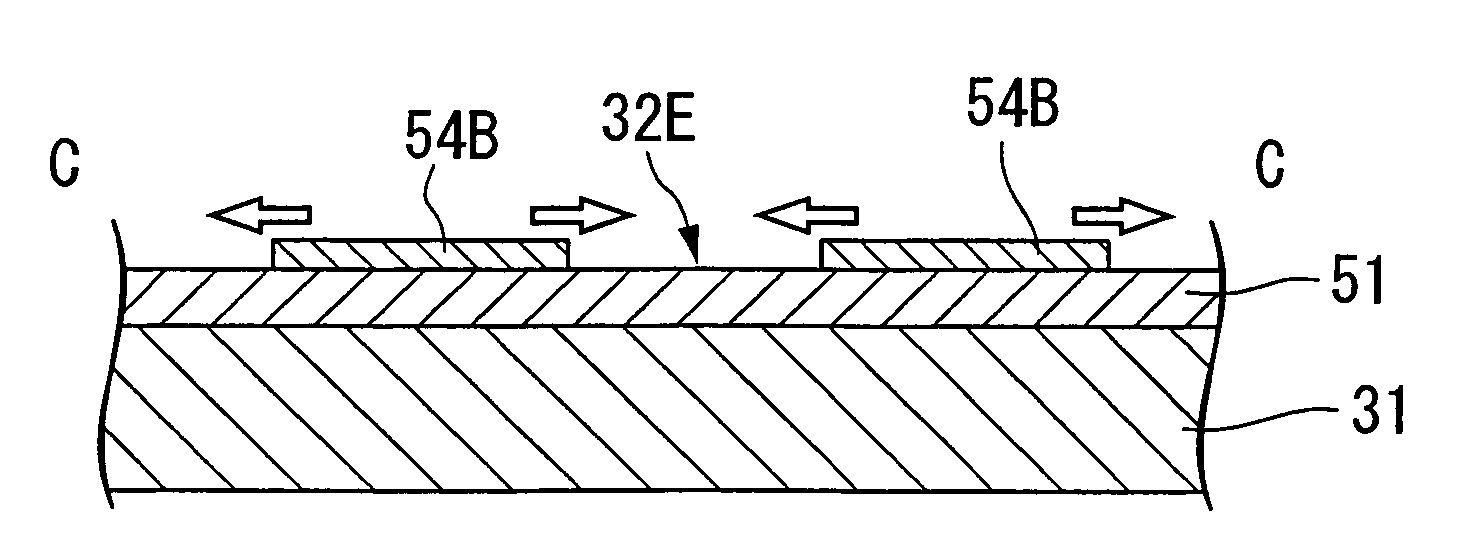
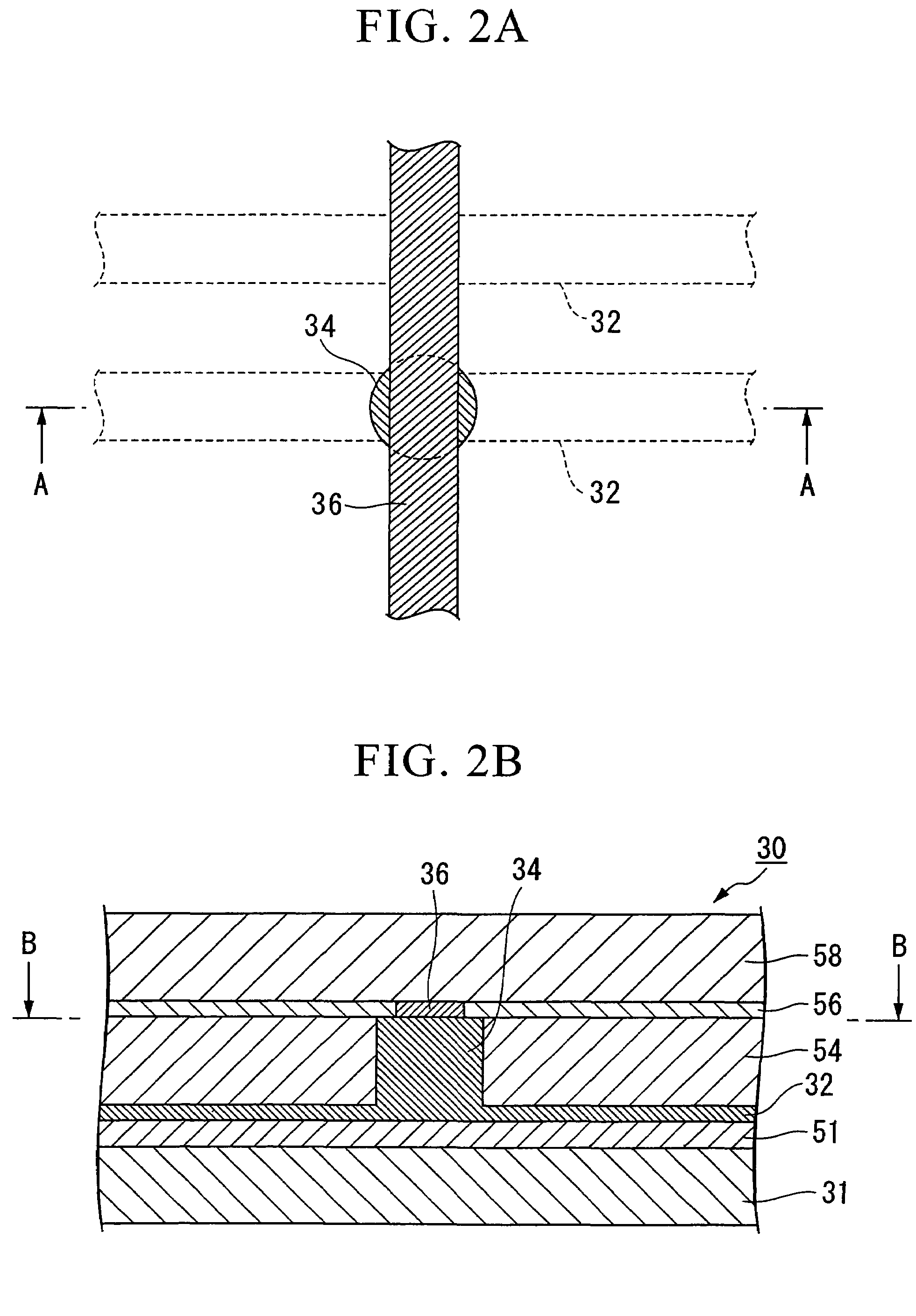
[0030]In the following, preferred embodiments of the present invention will be explained with reference to the drawings. In these drawings which are utilized in the following explanation, appropriate changes have been made in the scale of the various members, in order to represent them at scales at which they can be easily understood. Furthermore although, in these preferred embodiments, each of the various electrical wires is dealt with as a wiring pattern, in some cases, a plurality of electrical wires is referred to, all together, as a wiring pattern.

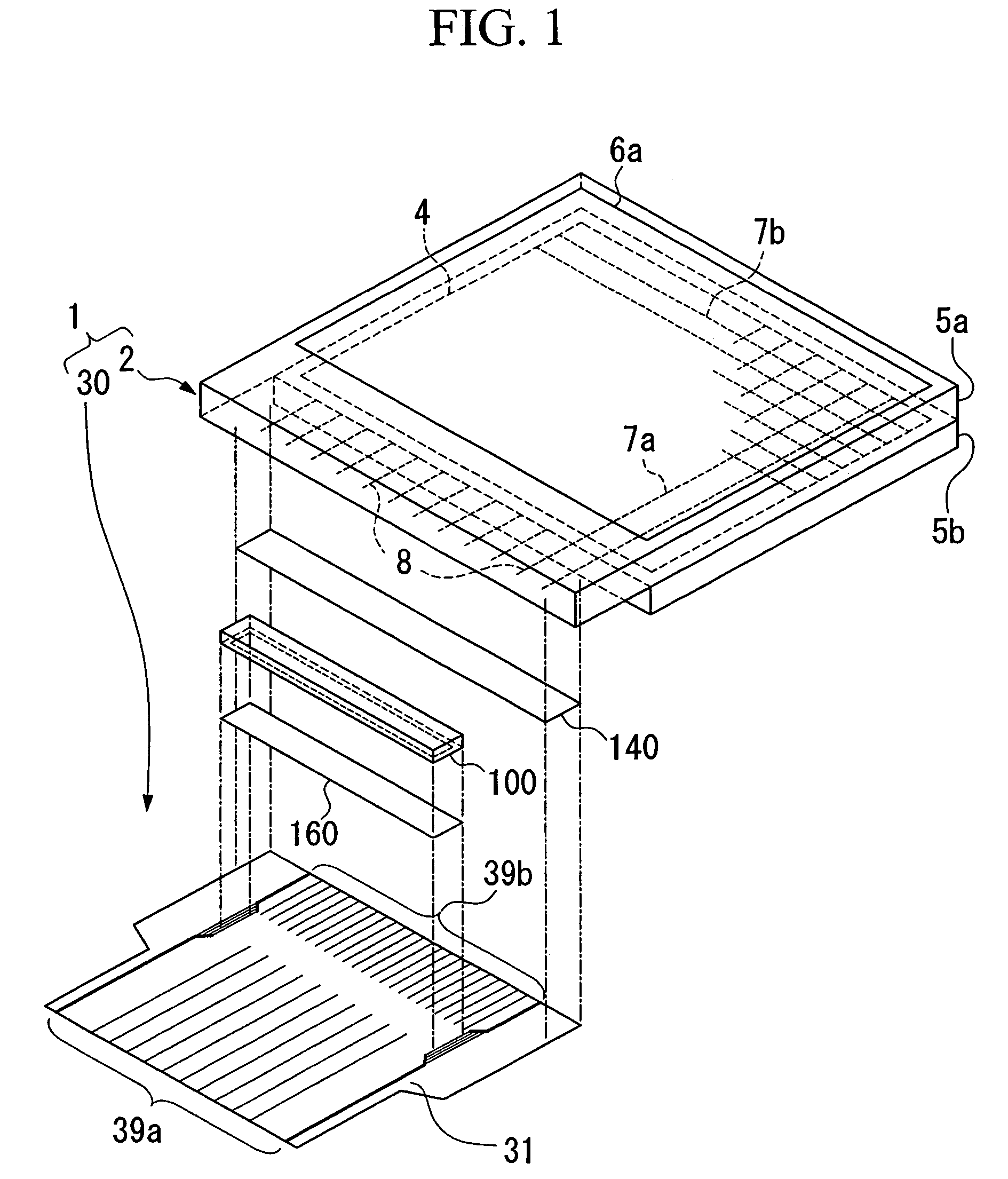
[0031]FIG. 1 is an exploded perspective view showing a liquid crystal module of a COF (Chip On Film) construction. In this preferred embodiment, by way of example, an example of a wiring pattern formation method for a flexible printed wiring substrate (Flexible Printed Circuit—hereinafter “FPC”) will be explained. This flexible printed wiring substrate includes a plurality of wiring layers which are mutually superimposed with insulat...


PUM

PropertyMeasurementUnit
wavelengthaaaaaaaaaa
widthaaaaaaaaaa
widthaaaaaaaaaa

Abstract

A wiring pattern formation method in which a wiring pattern is formed by arranging, in a region which is demarcated by a partition wall, liquid material which includes an electrically conductive material, including: arranging a resin material around the periphery of a region upon which the wiring pattern is to be formed; imparting liquid affinity to a demarcated region which has been demarcated by the resin material; narrowing down the demarcated region by flowing out the resin material towards and into the demarcated region; and forming the partition wall by curing the resin material.

Description

BACKGROUND OF THE INVENTION[0001]1. Field of the Invention[0002]The present invention relates to a wiring pattern formation method, a manufacturing method for a multi layer wiring substrate, and an electronic device.[0003]Priority is claimed on Japanese Patent Application No. 2004-282217, filed Sep. 28, 2004, the content of which is incorporated herein by reference.[0004]2. Description of Related Art[0005]In the manufacture of wiring or the like which is incorporated in an electronic circuit of an integrated circuit, for example, a lithographic method may be used. In such a lithographic method, there is a requirement for large scale equipment such as a vacuum device and complicated processing. Furthermore, with a lithographic method, the cost of manufacturing is high, since the efficiency of utilization of material is only around a few percent, and it is not possible to avoid throwing away almost all of this material. In this connection, as a process to be utilized instead of such a...

Claims


Application Information

Patent Timeline
Patent Type & Authority Patents(United States)
IPC IPC(8): H01L21/44
CPCC23C26/00H01L21/288H01L21/4867H05K3/125H05K3/1258G02F1/13452H01L21/76801H01L21/76825H01L21/76879H01L27/3297H05K3/4664H05K2201/09909H05K2203/013H05K2203/0568H10K59/179H05K3/10H05K3/46
Inventor UEHARA, NOBORUSHINTATE, TSUYOSHISAKURADA, KAZUAKI
Owner SEIKO EPSON CORP
Why Eureka
Try Eureka