
Circuit board and method of manufacturing the same

a technology of circuit boards and conductive patterns, applied in the field of circuit boards, can solve the problems of large impedances of conductive patterns for high-frequency signals, and achieve the effect of small impedances

Inactive Publication Date: 2007-11-06
PANASONIC CORP
View PDF7 Cites 10 Cited by
  • Summary
  • Abstract
  • Description
  • Claims
  • Application Information

AI Technical Summary

Benefits of technology

[0006]In this circuit board, the conductive layers have small impedances even if a high-frequency signal flows in the conductive layers.

Problems solved by technology

In the circuit boards including fine conductor patterns manufactured by the above methods, however, the conductor patterns may have large impedances for high-frequency signals.

Method used


Image

  • Circuit board and method of manufacturing the same
  • Circuit board and method of manufacturing the same
  • Circuit board and method of manufacturing the same

Examples


exemplary embodiment 1

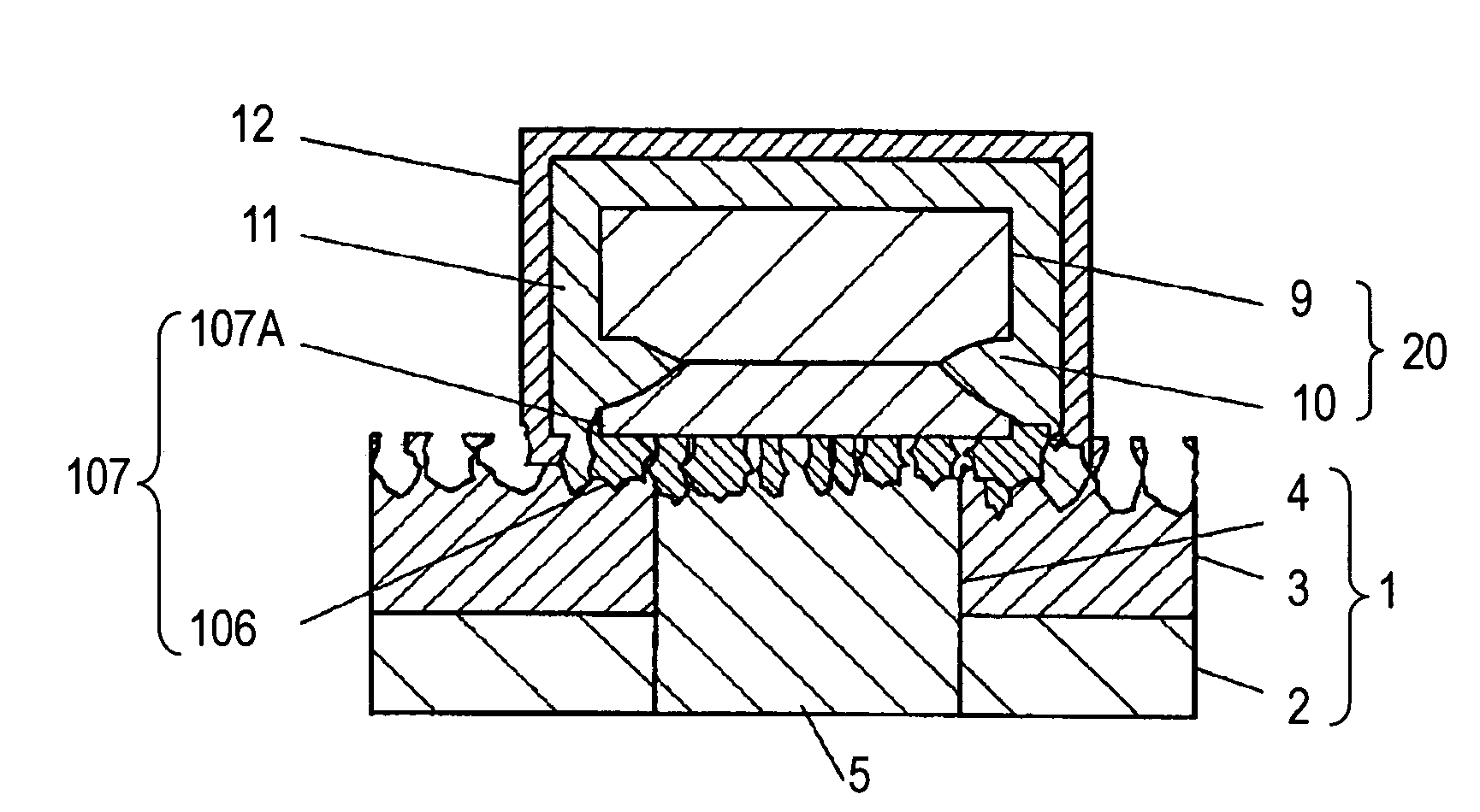
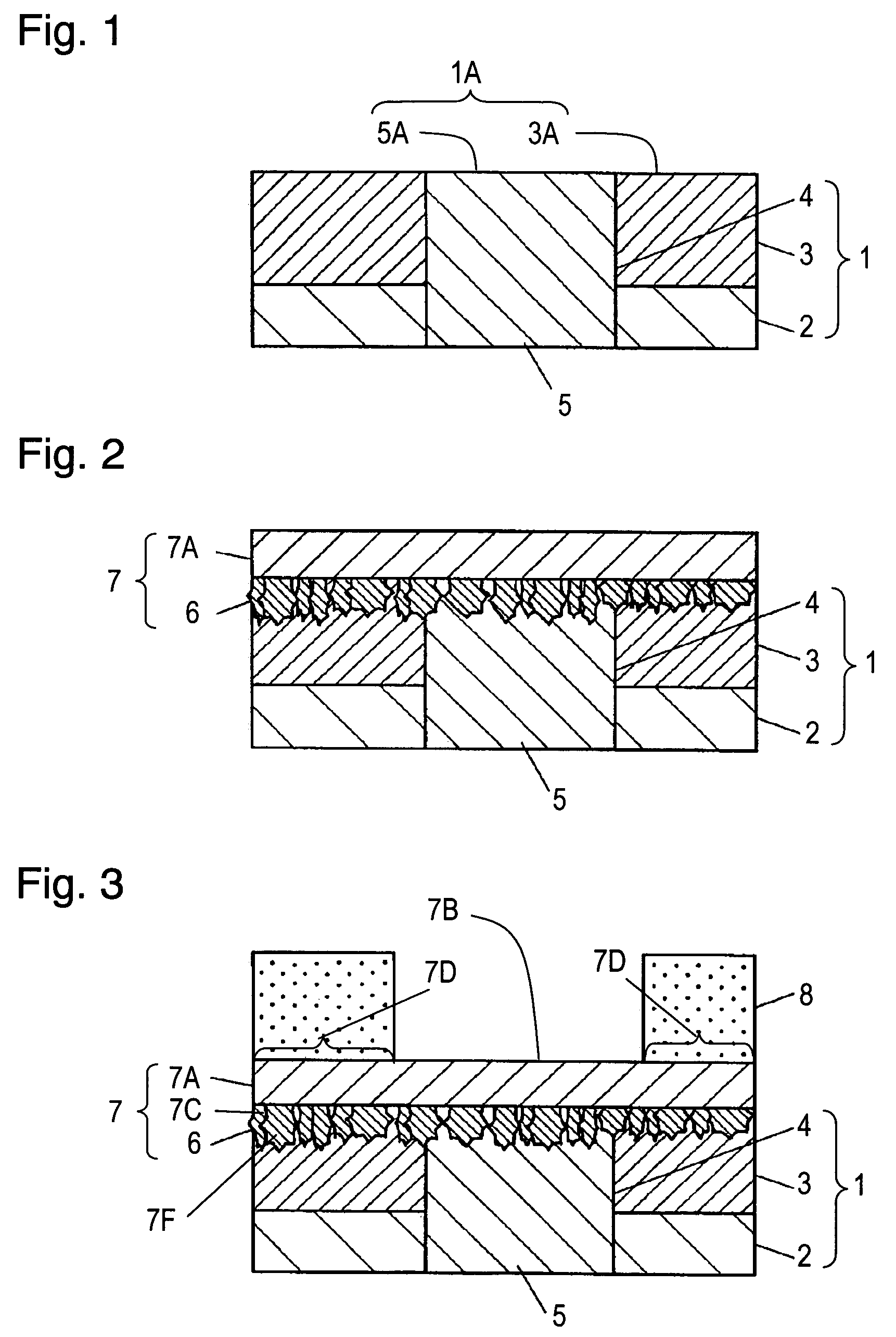
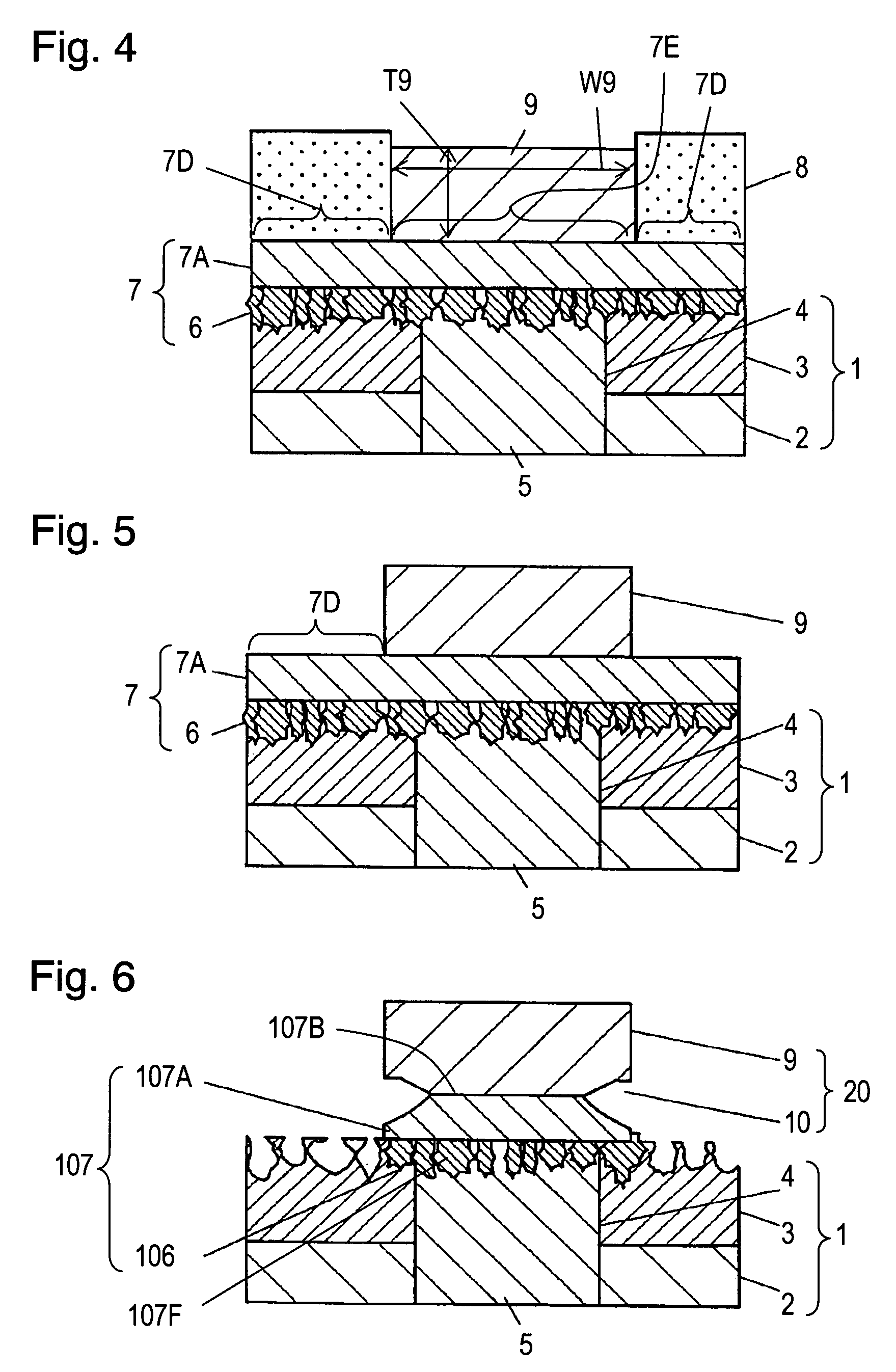
[0022]FIGS. 1 to 6 are cross sectional views of a circuit board for illustrating processes of manufacturing the circuit board according to Exemplary Embodiment 1 of the present invention.

[0023]FIG. 1 is a cross sectional view of insulating substrate 1 having through hole 4 filled with conductive material 5. Fiber sheet 2 of glass cloth (glass fabric) woven with insulating fiber, such as aramid resin fiber or glass fiber has both surfaces each impregnated with epoxy resin to provide resin layer 3 having a thickness ranging, for example, from 5 μm to 20 μm. Insulating substrate 1, or a glass epoxy substrate, is thus provided. Through-hole 4 is formed in insulating substrate 1 by optical process, such as CO2 gas laser, or a mechanical drill. Through-hole 4 is filled with a paste of electro conductive material 5 provided by mixing 30-80 vol. % of copper grains having diameters of 1 μm to 50 μm in a resin material for a 30-80 capacitive %, by printing process or injection.

[0024]Lateral a...

exemplary embodiment 2

[0047]FIGS. 8 to 15 are cross sectional views of a circuit board for illustrating a method of manufacturing the circuit board according to Exemplary Embodiment 2 of the present invention. Portions identical to those of Embodiment 1 are denoted by the same reference numerals, and description of the portions is eliminated.

[0048]First, as shown in FIG. 8, insulating substrate 1 formed by the same method as of the Embodiment 1 is provided with through-hole 4 by an optical method, such as CO2 gas laser or by a mechanical method, such as drilling. Through-hole 4 is filled with paste of electrical conductive material 5. Conductive material is provided by mixing 30 to 80 vol. % of copper grains having diameters ranging from 1 μm to 50 μm in resin material. The paste can be dispensed by printing process or jet nozzle injection.

[0049]As shown in FIG. 9, rough layer 506 is provided on surface of 501A of insulating substrate 1 by applying a roughening process, i.e., on surface 505A of conductiv...


PUM

PropertyMeasurementUnit
thicknessaaaaaaaaaa
diametersaaaaaaaaaa
diameteraaaaaaaaaa

Abstract

A circuit board includes an insulating substrate, a first conductive layer on the insulating substrate, a second conductive layer on the first conductive layer, and a third conductive layer covering the first conductive layer and the second conductive layer. The first conductive layer has a surface provided on the surface of the insulating substrate, and a surface having a width smaller than a width of the above surface. In this circuit board, the conductive layers have small impedances even if a high-frequency signal flows in the conductive layers.

Description

FIELD OF THE INVENTION[0001]The present invention relates to a circuit board including a conductive layer formed on an insulating substrate, and to a method for manufacturing the circuit board.BACKGROUND OF THE INVENTION[0002]In a conventional semi-additive method of manufacturing a circuit board which includes minute conductive layer, a first thin conductive layer is formed on an insulating substrate, and then a photosensitive resin shaped in a predetermined pattern is provided on the conductive layer. A second conductive layer is formed on a portion of the first conductive layer exposing from the photosensitive resin. After the photosensitive resin on the first conductive layer is removed to allow a portion of the first conductive layer to expose, and the exposing portion is etched off, thus providing the circuit board.[0003]In a method disclosed in Japanese Patent Laid-Open Publication No. 2004-95983, a first metal film is formed on the insulating substrate, and then the metal fi...

Claims


Application Information

Patent Timeline
Patent Type & Authority Patents(United States)
IPC IPC(8): H01L23/48H01L23/52H01L29/40
CPCH05K3/108H05K3/24H05K1/0242H05K1/0237Y10T29/49126H05K3/181H05K3/381H05K3/383H05K3/384H05K3/4069H05K2201/0338H05K2201/0355H05K2201/098H05K2203/0307H05K2203/0392Y10T29/49133Y10T29/49128
Inventor SUGAWA, TOSHIOHIGASHITANI, HIDEKIMISAKI, TAKUMI
Owner PANASONIC CORP
Learn More