Eureka AIR delivers breakthrough ideas for toughest innovation challenges, trusted by R&D personnel around the world.

Communication semiconductor integrated circuit device and wireless communication system

a technology of integrated circuits and semiconductors, applied in the direction of electrically long antennas, antennas, electrical equipment, etc., can solve the problems of increasing chip size, degrading the modulator modulation accuracy, and increasing the distortion of transmission signals, so as to reduce the chip size and prevent the degrading of transmission signals

Inactive Publication Date: 2007-07-03
RENESAS ELECTRONICS CORP
View PDF13 Cites 18 Cited by
  • Summary
  • Abstract
  • Description
  • Claims
  • Application Information

AI Technical Summary

Benefits of technology

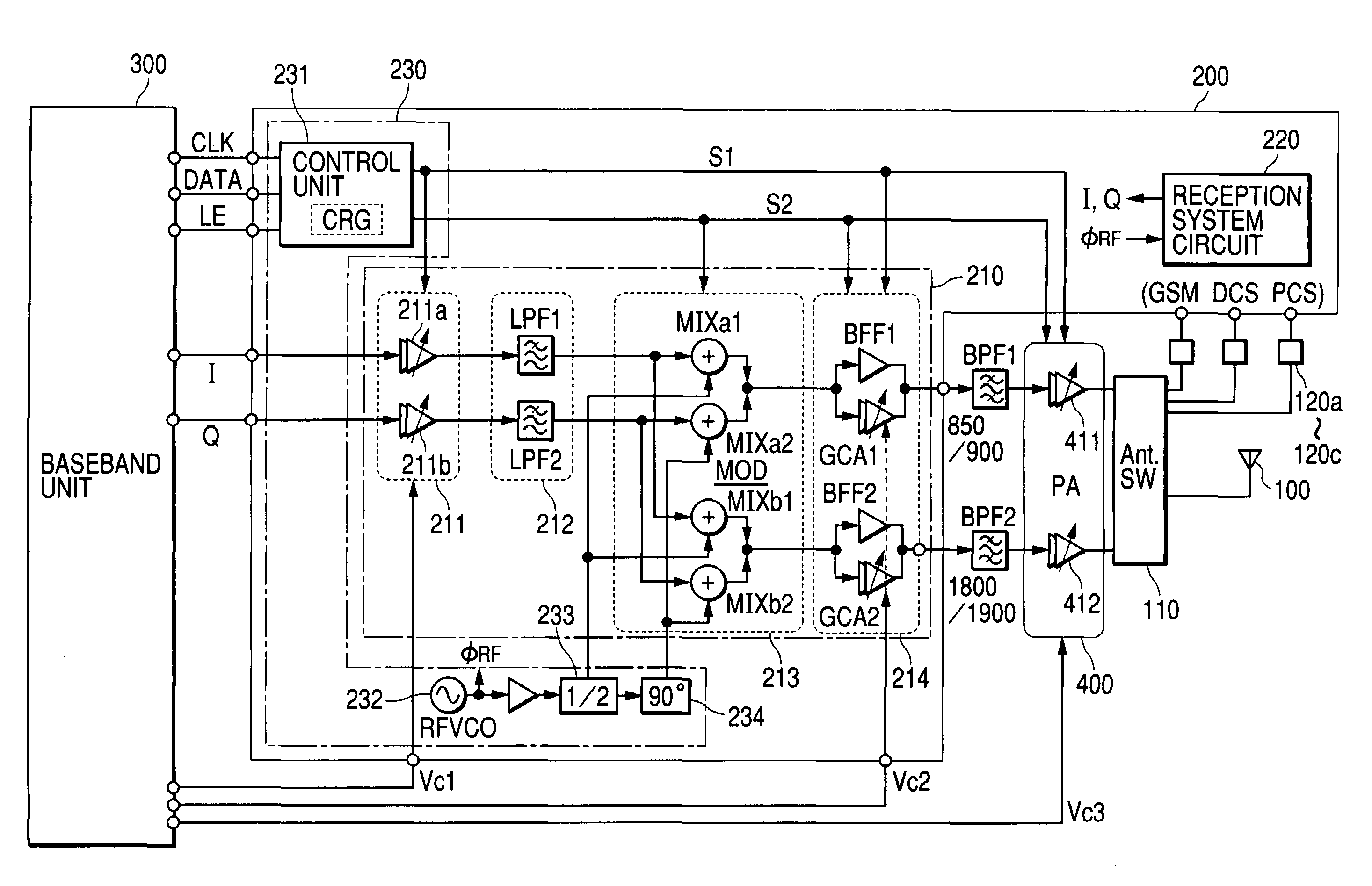
[0018]An object of the present invention is to provide a communication semiconductor integrated circuit device capable of transmission in two or more modulation modes and outputting transmission signals with less distortion.
[0019]Another object of the present invention is to provide a communication semiconductor integrated circuit device which is capable of transmission in two or more modulation modes and allows reduction in size.
[0020]A further object of the present invention is to provide a communication semiconductor integrated circuit device capable of transmission in two or more modulation modes and with less leakage power to the reception band or adjacent channels.
[0024]According to the above-mentioned means, unwanted waves produced by signal interference between circuits or gain control in a gain variable amplification circuit can be reduced. Thus, a transmission signal with high modulation accuracy and less distortion can be outputted, and leakage power to the reception band or adjacent channels can be reduced.
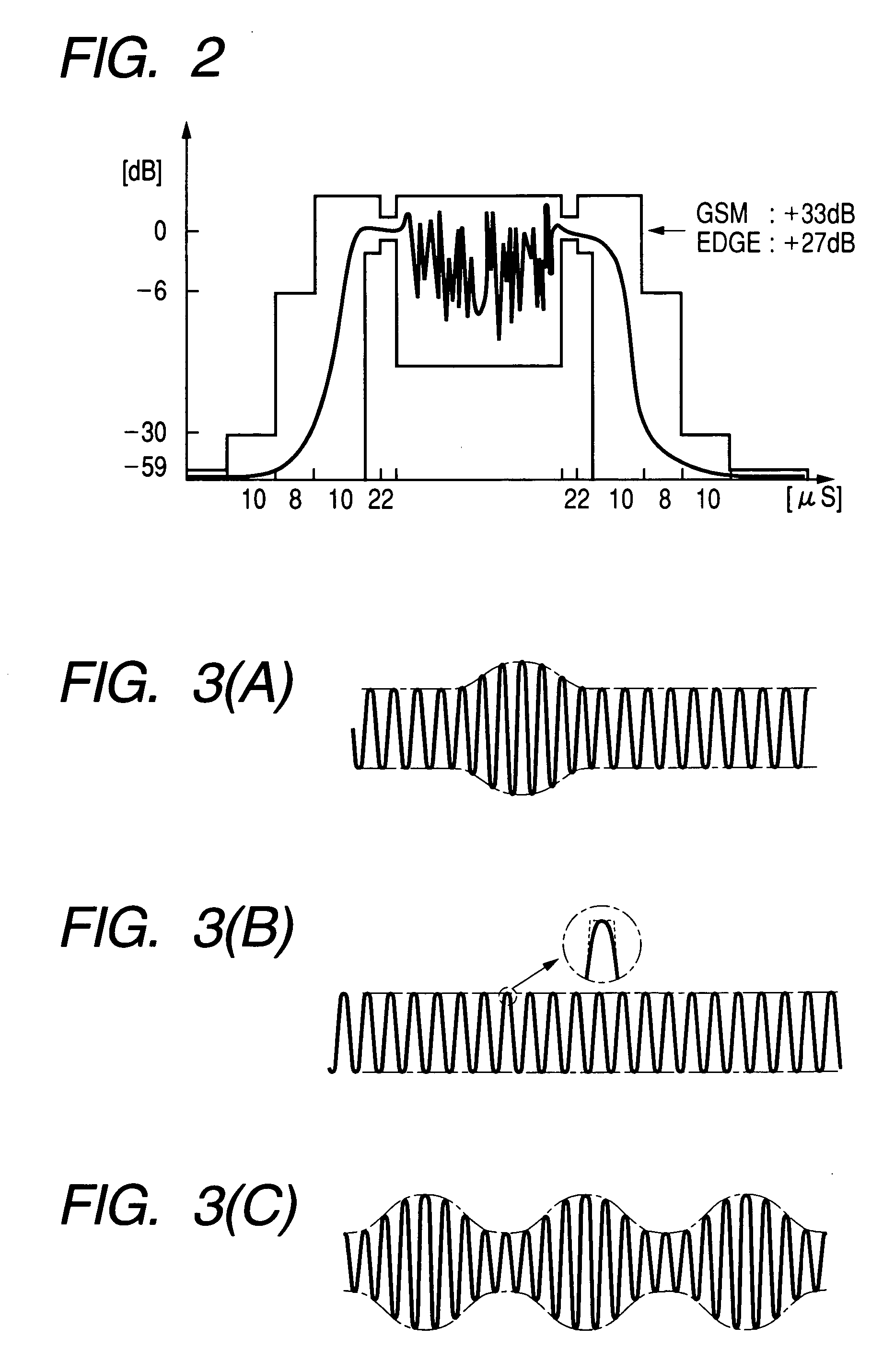
[0026]As a result, a circuit provided with a modulating function and a frequency converting function can be used in common in transmissions in different frequency bands, and thus the chip size can be reduced. Further, this prevents amplitude distortion from being converted into phase distortion through the power amplification circuit in the later stage in GSM mode and thus the accuracy of transmission signals from being degraded.

Problems solved by technology

However, when a frequency converter and a gain variable amplifier are formed over the same semiconductor chip as a modulator is, a problem arises.
For example, if a gain variable amplifier is not favorable in linear characteristics, a problem arises.
Therefore, the modulation accuracy of a modulator is degraded, or distortion in a transmission signal is increased.
Therefore, even if they are formed over one semiconductor chip, a problem of increased chip size results.

Method used


Image

  • Communication semiconductor integrated circuit device and wireless communication system
  • Communication semiconductor integrated circuit device and wireless communication system
  • Communication semiconductor integrated circuit device and wireless communication system

Examples


second embodiment

[0057]FIG. 4 illustrates an example of the configuration of the high frequency IC in the present invention and a wireless communication system using it.

[0058]In the second embodiment, the buffers BFF1 and BFF2 having a limiter function in the first embodiment are omitted. Instead, only the gain variable amplifiers GCA1 and GCA2 are provided as the second amplifying unit 214 in the stage subsequent to the modulating-frequency converting unit 213. For the rest, the constitution is the same as that of the first embodiment. In this embodiment, modulated signals are amplified and outputted by the gain variable amplifier GCA1 and GCA2 in GSM mode as well as in EDGE mode.

[0059]The second embodiment obviates the buffers BFF1 and BFF2. Therefore, in the second embodiment, the scale of the circuitry is accordingly reduced as compared with the embodiment in FIG. 1, and the chip size can be reduced. Further, the first amplifying unit 211, filter unit 212, and modulating-frequency converting uni...

first embodiment

[0061]Further, band-pass filters having more favorable characteristic than BPF1 and BPF2 in the first embodiment may be used as the band-pass filters BPF1 and BPF2 in the later stage. Thus, without use of the buffers BFF1 and BFF2 having a limiter function, transmission signals with relatively less distortion can be similarly inputted to the power module 400 in GSM mode.

third embodiment

[0062]FIG. 5 illustrates an example of the configuration of the high frequency IC in the present invention and a wireless communication system using it.

[0063]In the third embodiment, the gain variable amplifiers GCA1 and GCA2 in the second embodiment are omitted. Instead, the third embodiment is provided with linear amplifiers AMP1 and AMP2 of fixed gain as the second amplifying unit 214 in the stage subsequent to the modulating-frequency converting unit 213. For the rest, the constitution is the same as that of the second embodiment. In this embodiment, the output level is raised by controlling the gain of the gain variable amplifiers 211a and 211b in the first amplifying unit 211 at start of transmission in GSM mode as well as in EDGE mode.

[0064]The third embodiment requires gain variable amplifiers 211a and 211b of a wider range of gain variation than in the first embodiment. However, the buffers BFF1 and BFF2 are unnecessary, and the scale of the circuitry is accordingly reduced...


PUM


Abstract

A communication semiconductor integrated circuit device is capable of transmission in two or more different modulation modes and outputting transmission signals with less distortion. The communication semiconductor integrated circuit device comprises a gain variable amplification circuit which amplifies I-signals and Q-signals; and a mixer circuit which synthesizes the amplified I-signals and Q-signals and local oscillation signals to carry out modulation and frequency conversion. The communication semiconductor integrated circuit device is capable of transmission in two or more different modulation methods, for example, in GSM mode and EDGE mode. A low-pass filter of second or higher order is placed between the gain variable amplification circuit and the mixer circuit.

Description

CROSS-REFERENCE TO RELATED APPLICATION[0001]The present application claims priority from Japanese patent application JP 2003-133875 filed on Mar. 13, 2003, the content of which is hereby incorporated by reference into this application.BACKGROUND OF THE INVENTION[0002]The present invention relates to a technology which is effectively applied to a transmitter circuit in a communication semiconductor integrated circuit device constituting a wireless communication system and further a transmitter circuit of such a modulation method that phase modulation and amplitude modulation are carried out. More particularly, the present invention relates to a technology effectively utilized in a transmitter circuit of direct up conversion type wherein a modulator which carries out modulation into an oscillation signal (carrier wave) on a predetermined frequency by I-signal and Q-signal carries out direct conversion into transmission frequency.[0003]Conventionally, various cellular phones have been ...

Claims


Application Information

Patent Timeline
IPC IPC(8): H04B1/04H04B1/707H04B1/40H04J13/00
CPCH04B1/005H04B1/0057H04B1/406
Inventor MATSUI, HIROAKIHORI, KAZUAKI
Owner RENESAS ELECTRONICS CORP
Why Eureka
Eureka Blog
Learn More