Method for forming a single crystalline film
a technology of crystalline film and crystalline structure, which is applied in the direction of crystal growth process, polycrystalline material growth, chemically reactive gas, etc., can solve the problems of insufficient technique for use in a real semiconductor manufacturing site, difficult to form a uniform film on a large-scale substrate,
- Summary
- Abstract
- Description
- Claims
- Application Information
AI Technical Summary
Benefits of technology
Problems solved by technology
Method used
Image

Examples
example 1
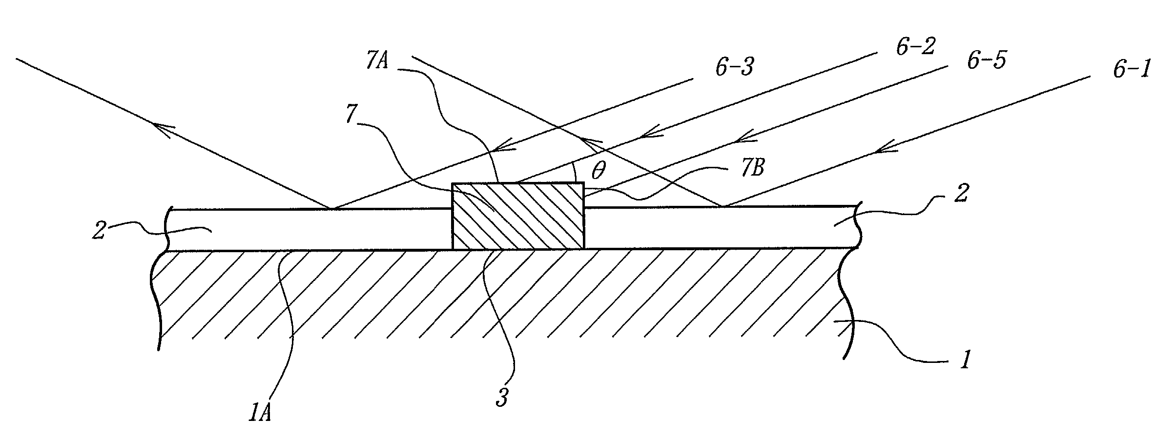
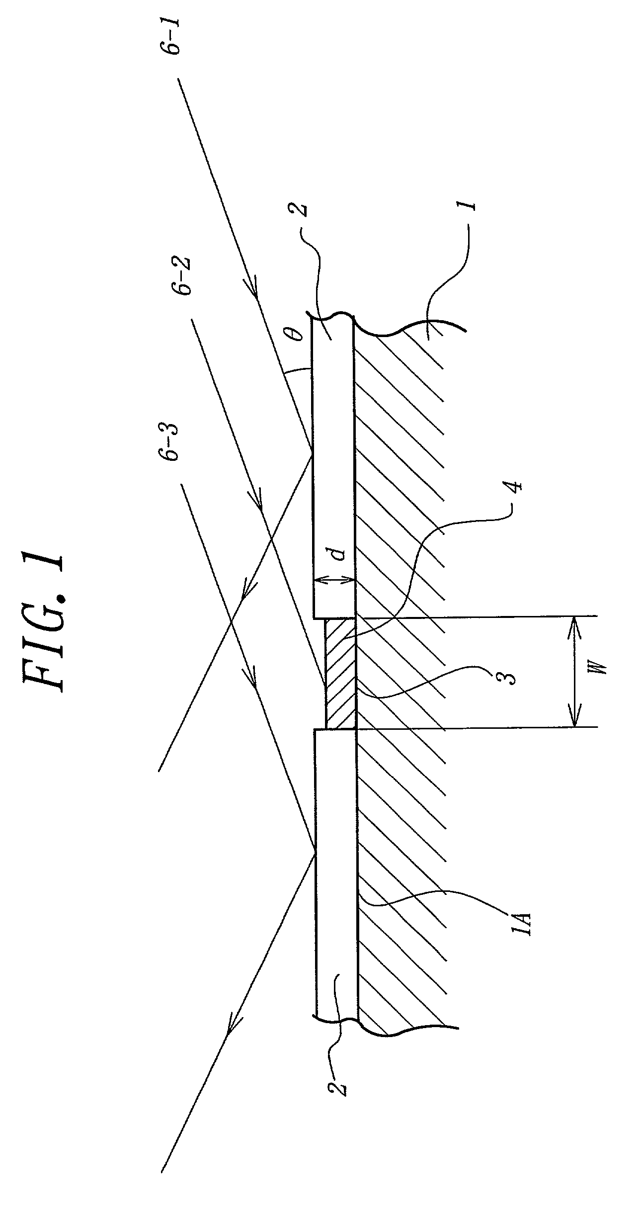
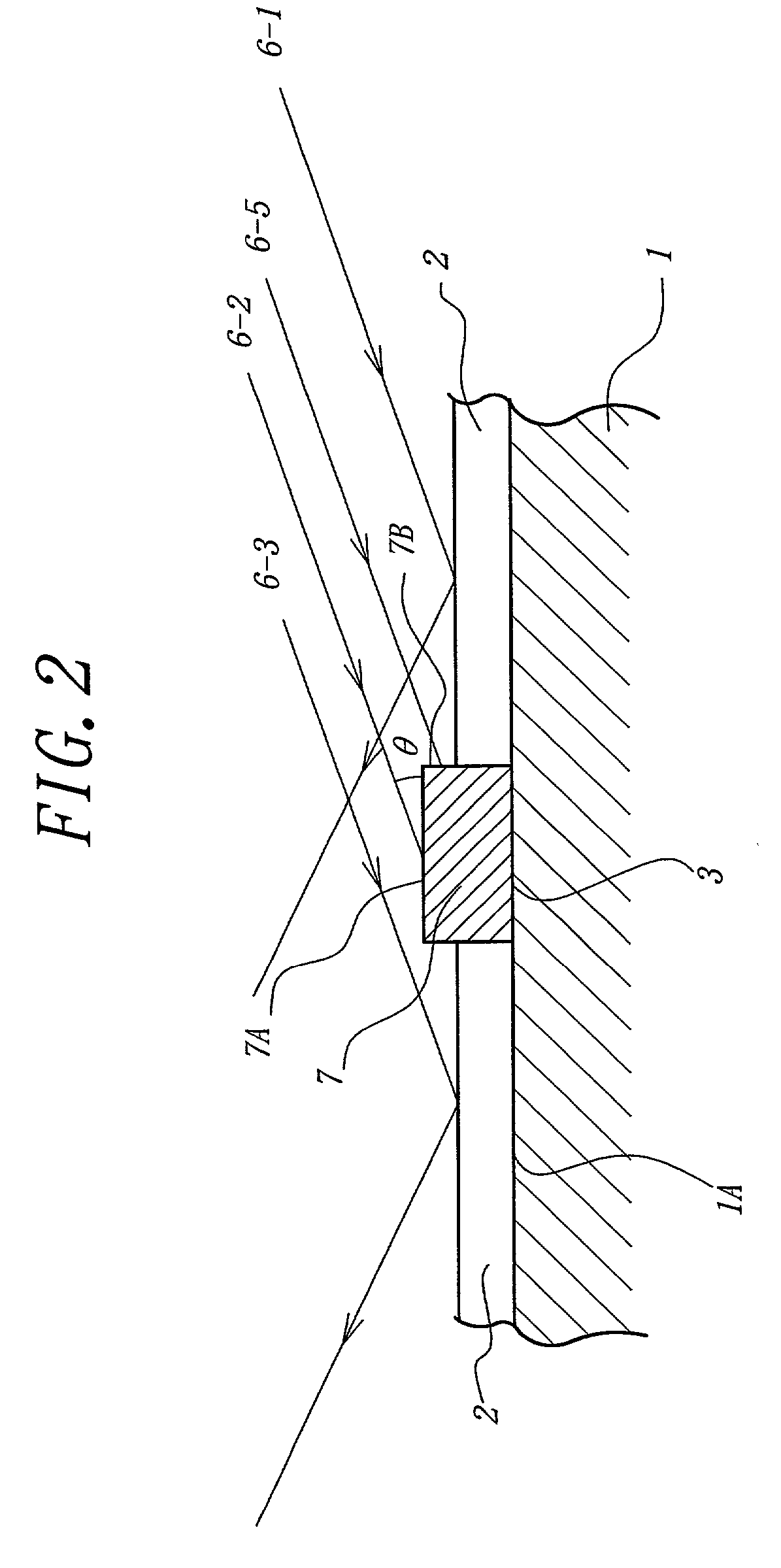
[0050]A silicon oxide film was formed in a thickness of 200 nm on a silicon single crystalline substrate having a diameter of 50 mm and a thickness of 0.5 mm by a plasma CVD method. Then, a linear opening having a width of 1 μm as shown in FIG. 1 was formed by photolithography to expose a part of a surface of the substrate.
[0051]After oxide films in the exposed surface of the substrate were removed by heating, SiH4 molecular beams were introduced onto the surface of the substrate at their incident angle of 20 degrees by using a gas source-molecular beam epitaxy equipment with the substrate being kept at a temperature of 950° C. Then, the decomposed Si atoms were selectively and epitaxially grown in the openings to form a single crystalline film therein.
[0052]Thereafter, when the epitaxial growth was continued by successively introduction of the molecular beams, the epitaxial growth occurred in a direction parallel to the surface of the substrate to form a single crystalline film on ...
example 2
[0054]Except that silicon atomic beams were introduced onto the silicon single crystalline substrate with mask at their incident angle of 10 degrees by an ultra-high vacuum molecular beam epitaxy equipment, the growth was carried out as described in Example 1.
[0055]A single crystalline film formed on the silicon oxide film had a thickness of 0.2 μm. Moreover, when the film was characterized by a reflection high energy electron diffraction, it turned out that the film was composed of silicon single crystal. When the film was chemically etched, etch-pits did not appear in the film. Then, the film was characterized by a transmission electron microscope and the dislocation density of the film was found not more than 102 / cm2.
example 3
[0056]Except that a Ta film having a thickness of 20 nm instead of the silicon oxide film was formed, the growth was carried out as described in Example 1.
[0057]A single crystalline film formed on the Ta film had a thickness of 0.2 μm. The film was investigated by a reflection high energy electron diffraction. It turned out that the film was composed of silicon single crystal. When the film was chemically etched, etch-pits did not appear in the film. Then, the film was characterized by a transmission electron microscope and the dislocation density of the film was found not more than 102 / cm2.
[0058]Except that a Ta film having a thickness of 20 nm instead of the silicon oxide film was formed, the growth was carried out as described in Example 2.
[0059]A single crystalline film formed on the Ta film had a thickness of 0.2 μm. The film was investigated by a reflection high energy electron diffraction. It turned out that the film was composed of silicon single crystal. When the film was c...
PUM
| Property | Measurement | Unit |
|---|---|---|
| incident angle | aaaaa | aaaaa |
| incident angle | aaaaa | aaaaa |
| width | aaaaa | aaaaa |
Abstract
Description
Claims
Application Information
 - R&D
- Intellectual Property
- Life Sciences
- Materials
- Tech Scout
- Unparalleled Data Quality
- Higher Quality Content
- 60% Fewer Hallucinations
Browse by: Latest US Patents, China's latest patents, Technical Efficacy Thesaurus, Application Domain, Technology Topic, Popular Technical Reports.
© 2025 PatSnap. All rights reserved.Legal|Privacy policy|Modern Slavery Act Transparency Statement|Sitemap|About US| Contact US: help@patsnap.com