Co-sputter deposition of metal-doped chalcogenides

a technology of metal-doped chalcogenides and co-sputtering, which is applied in the field of memory technology, can solve the problems of nonvolatile memory devices that retain data, lose data, and loss of data, and achieve the effect of high degree of depth-profile uniformity and precise and efficient control of constituent ratios

Inactive Publication Date: 2007-04-10
ROUND ROCK RES LLC
View PDF219 Cites 4 Cited by
  • Summary
  • Abstract
  • Description
  • Claims
  • Application Information

AI Technical Summary

Benefits of technology

[0012]Embodiments of the present invention include systems and methods that overcome the disadvantages of the prior art. The systems and methods described herein allow a chalcogenide glass, such as germanium selenide (GexSe1-x), to be doped with a metal such as silver (Ag), copper (Cu), and zinc (Zn), without utilizing an ultraviolet (UV) photodoping step to dope the chalcogenide glass with the metal. Other examples of chalcogenide glasses that can be used include germanium sulfide (GexSe1-x) and arsenic selenide (AsxSe1-x). Advantageously, embodiments of the invention co-sputter the metal and the chalcogenide glass and allow for relatively precise and efficient control of a constituent ratio between the doping metal and the chalcogenide glass. Further advantageously, the systems and methods enable the doping of the chalcogenide glass with a relatively high degree of depth-profile uniformity. Also, the systems and methods allow a metal concentration to be varied in a controlled manner along the thin film depth.

Problems solved by technology

A volatile memory loses its data when power is removed.
In addition, certain volatile memories such as DRAM devices require periodic refresh cycles to retain their data even when power is continuously supplied.
In contrast to the potential loss of data encountered in volatile memory devices, nonvolatile memory devices retain data for long periods of time when power is removed.
Disadvantageously, the photodoping process is relatively time-consuming and can slow semiconductor fabrication rates.
The photodoping process can decrease the overall process rate especially when it is repetitively applied, such as in the fabrication of a multiple layer stack.
Further disadvantageously, the extended exposure to intense UV radiation can induce the glass to convert from an amorphous material to a crystallized material, which thereby results in reduced yields.
Another disadvantage to producing memory cells with silver (Ag) photodoping of glasses is that relatively precise control of the amount of silver (Ag) that is photodiffused into the glass is necessary.
If too little silver (Ag) were to be photodiffused into the glass, the memory cell would not switch properly.
Another disadvantage to the photodoping process is that the ultraviolet light is attenuated by the silver film as the ultraviolet light penetrates through the silver film.
This attenuation renders photodoping to be impractical with relatively thick films, and requires relatively precise control of the thicknesses of the silver (Ag) and chalcogenide glass films.
In order to form a thick film with a UV photodoping process, the UV photodoping process is disadvantageously applied repetitively to relatively thin films of silver (Ag).
Further disadvantageously, this attenuation in intensity of the ultraviolet light as the ultraviolet light penetrates material results in a non-uniform depth profile of the doped silver (Ag) in the chalcogenide glass.

Method used


Image

  • Co-sputter deposition of metal-doped chalcogenides
  • Co-sputter deposition of metal-doped chalcogenides
  • Co-sputter deposition of metal-doped chalcogenides

Examples


Embodiment Construction

[0025]Although this invention will be described in terms of certain preferred embodiments, other embodiments that are apparent to those of ordinary skill in the art, including embodiments which do not provide all of the benefits and features set forth herein, are also within the scope of this invention. Accordingly, the scope of the present invention is defined only by reference to the appended claims.

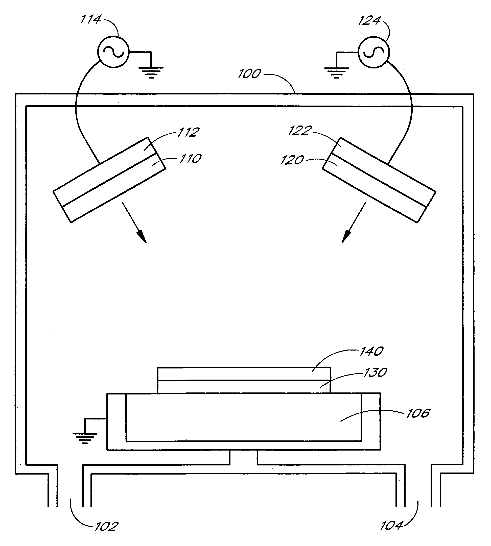
[0026]Embodiments of the present invention allow a chalcogenide glass such as germanium selenide (GexSe1-x) to be doped with a metal such as silver (Ag), copper (Cu), or zinc (Zn) without the performance of an ultraviolet (UV) photodoping step. Other examples of chalcogenide glasses that can be used include germanium sulfide (GexSe1-x) and arsenic selenide (AsxSe1-x). The value of x can vary in a wide range. Although the value of x can theoretically range from 0 to 1, the fabrication of a programmable conductor random access memory (PCRAM) should maintain the value of x such that the u...


PUM

PropertyMeasurementUnit
volatileaaaaaaaaaa
poweraaaaaaaaaa
electric fieldaaaaaaaaaa

Abstract

The present invention is related to methods and apparatus that allow a chalcogenide glass such as germanium selenide (GexSe1-x) to be doped with a metal such as silver, copper, or zinc without utilizing an ultraviolet (UV) photodoping step to dope the chalcogenide glass with the metal. The chalcogenide glass doped with the metal can be used to store data in a memory device. Advantageously, the systems and methods co-sputter the metal and the chalcogenide glass and allow for relatively precise and efficient control of a constituent ratio between the doping metal and the chalcogenide glass. Further advantageously, the systems and methods enable the doping of the chalcogenide glass with a relatively high degree of uniformity over the depth of the formed layer of chalcogenide glass and the metal. Also, the systems and methods allow a metal concentration to be varied in a controlled manner along the thin film depth.

Description

RELATED APPLICATION[0001]This application is related to the disclosure of U.S. application Ser. No. 10 / 164,646 of Li et al., filed Jun. 6, 2002, entitled ELIMINATION OF DENDRITE FORMATION DURING METAL / CHALCOGENIDE GLASS DEPOSITION, the entirety of which is hereby incorporated by reference.CROSS REFERENCE TO RELATED APPLICATIONS[0002]This application is a divisional of U.S. patent application Ser. No. 10 / 164,429, filed Jun. 6, 2002, now U.S. Pat. No. 6,890,790 entitled CO-SPUTTER DEPOSITION OF METAL DOPED CHALCOGENIDES, the entire disclosure of which is hereby incorporated by reference.BACKGROUND OF THE INVENTION[0003]1. Field of the Invention[0004]The present invention generally relates to memory technology. In particular, the present invention relates to the fabrication of metal-doped chalcogenides.[0005]2. Description of the Related Art[0006]Computers and other digital systems use memory to store programs and data. A common form of memory is random access memory (RAM). Many memory...

Claims


Application Information

Patent Timeline
Patent Type & Authority Patents(United States)
IPC IPC(8): H01L21/00C23C14/06C23C14/34C23C14/54H01L45/00
CPCC23C14/0623C23C14/3464C23C14/548H01L45/085H01L45/1233H01L45/142H01L45/143H01L45/1625H10N70/245H10N70/826H10N70/8822H10N70/8825H10N70/026
Inventor LI, JIUTAOMCTEER, ALLENHERDT, GREGORYDOAN, TRUNG T.
Owner ROUND ROCK RES LLC
Why Eureka
Try Eureka