
Multiplier-based processor-in-memory architectures for image and graphics processing

a multi-core processor and image processing technology, applied in the field of processor-in-memory architectures for image and graphics processing, can solve the problems of architectures experiencing bottlenecks, large computing power demand, and large computing power consumption of these devices, and achieves low cost, low cost, and high controllability and observability. high

Inactive Publication Date: 2007-01-23
UNIVERSITY OF ROCHESTER +2
View PDF6 Cites 81 Cited by
  • Summary
  • Abstract
  • Description
  • Claims
  • Application Information

AI Technical Summary

Benefits of technology

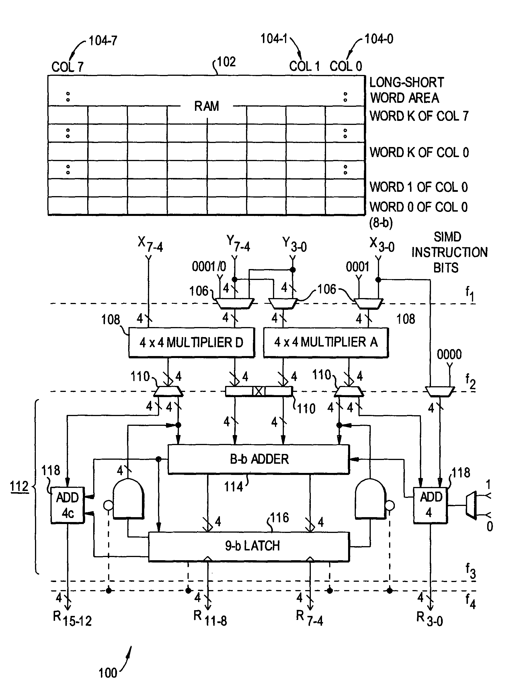
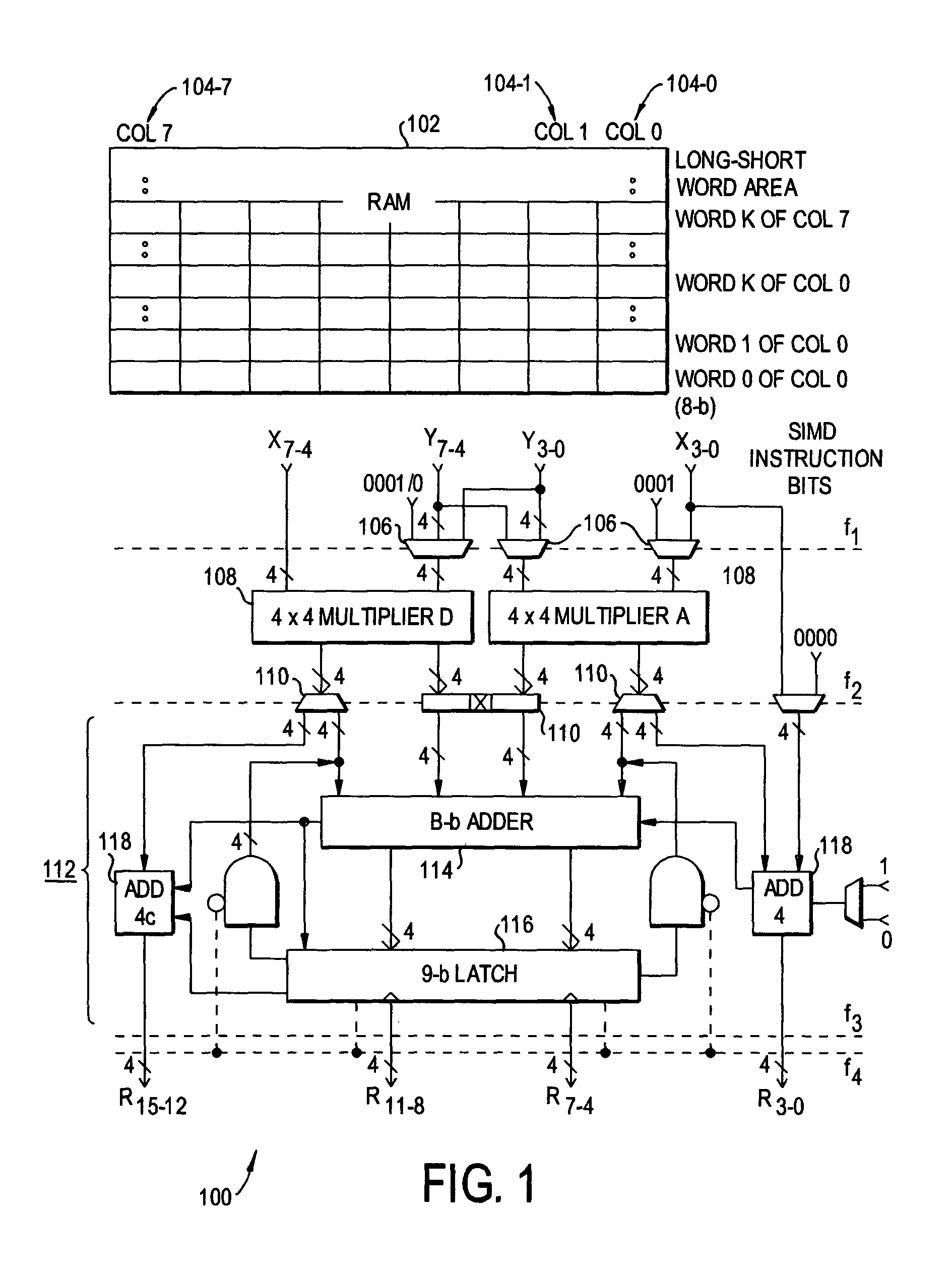
[0022]The PIM comprises an array of small multipliers (for example, 210 4×4 multipliers), which can be dynamically reconfigurable for 8-b and 16-b add, subtract, compare and multiply operations, as well as for vector-vector and matrix-vector multiplications, all in SIMD parallel form. The PIM can be implemented as an SRAM having grouped pixel columns, or grouped voxel columns. Both the ALU and the SRAM are scalable and can be easily extended.
[0027]The PIM architectures according to the present invention have a major advantage over the well-known designs: the capability of trading (or decomposing) bitwidth of operands for the size of the array to be processed. The trading can take place not only at software level, but also at hardware level.
[0029]One embodiment of the present invention provides a highly regular self-repairable and reconfigurable 16×16-b parallel multiplier / inner product processor along with a low-power fast CMOS circuit implementation and an exhaustive DFT method. The circuit can be efficiently reconfigured into 17 different architectures, recovering the specified faults over 52% of the transistors. Both the repairing and testing take the advantage of the clean partitioning of the circuit, which results in high controllability and observability, inherent in the decomposition approach. The processor can be directly extended for operations in twos complement form, with a negligible amount of VLSI area increase. The repairing coverage can be extended to allow one fault mid-final adder and one fault 4-bit group adder in the final adder to be recovered, which provides 17*5*5=425 different architectures for repairing. This would recover the specified faults for almost all transistors in the circuit. However, the additional VLSI area (transistors and, particularly, lines), the delay (5 ns) and test vector length (1.5*217) needed are non-proportionally larger, mainly due to that all component inputs must be collected, instead of generated.

Problems solved by technology

This leads to greater demand for computing power, but at the same time, the size, weight, and power consumption of these devices must remain constant.
In addition to high complexity, which results in a large area overhead (30–70%), these architectures experience bottlenecks in increased leakages of the DRAM due to a very high temperature dissipation of the processing elements.
As a result, the retention frequency will have to be increased, and that will push the power consumption levels even higher.
Lastly, the testing cost of the stand-alone DRAM is already high, and adding a microprocessor to it could increase the test time, and thereby costs, significantly.
The main disadvantage of such a simple PE is that operations such as multiplication require significantly more memory accesses to store intermediate results.
Therefore, the multiplication operation has small performance and increased power consumption.
The latency for multiplication is reduced because of the reduced number of RAM cycles; however, it does not provide sufficient throughput for multimedia support.
Finally, both designs are implemented using dynamic logic, which results in higher power consumption due to the precharge phase within every cycle.
Due to its complexity, it has a very large area overhead, and the implementation would not be cost effective.
This approach has, therefore, severe limitations for image and graphics applications.
First, the dynamic logic implementation has high power consumption, and therefore, it would be difficult for use in a portable environment.
Secondly, the PE is very inefficient in performing multiplication operations.
While it can perform operations such as Add, Compare, Shift, Accumulate, with high throughput, the architecture lacks several orders of magnitude behind in multiplication.

Method used


Image

  • Multiplier-based processor-in-memory architectures for image and graphics processing
  • Multiplier-based processor-in-memory architectures for image and graphics processing
  • Multiplier-based processor-in-memory architectures for image and graphics processing

Examples


Embodiment Construction

[0041]Preferred embodiments of the present invention will be set forth in detail with reference to the drawings, in which like reference numerals refer to like elements throughout. The first preferred embodiment provides both a new arithmetic scheme for ALU design and a new digital accelerator architecture for implementing that arithmetic scheme. The second preferred embodiment adds self-repair capabilities.

[0042]The arithmetic scheme has the following characteristics:

[0043]1. It uses small multipliers (ex. 4×4-b) instead of full-adder and / or other parallel counters as building blocks. That provides greater flexibility for enlarging functionality through reconfiguration.

[0044]2. It enables multipliers directly dealing with wider sense arithmetic operations including:[0045]a family of multiplications: 8×8-b, 16×16-b, 32×32-b, vector×vector, and vector×matrix, i.e. size-4 vector and size 4×4 matrix products; and[0046]merged arithmetic operations including addition, subtraction, compar...


PUM


Abstract

A Procesor-In-Memory (PIM) includes a digital accelerator for image and graphics processing. The digital accelerator is based on an ALU having multipliers for processing combinations of bits smaller than those in the input data (e.g., 4×4 adders if the input data are 8-bit numbers). The ALU implements various arithmetic algorithms for addition, multiplication, and other operations. A secondary processing logic includes adders in series and parallel to permit vector operations as well as operations on longer scalars. A self-repairing ALU is also disclosed.

Description

REFERENCE TO RELATED APPLICATIONS[0001]The present application claims the benefit of U.S. Provisional Application Nos. 60 / 370,722 and 60 / 370,723, both filed Apr. 9, 2002, whose disclosures are hereby incorporated by reference in their entireties into the present disclosure.STATEMENT OF GOVERNMENT INTEREST[0002]The work leading to the present application was supported, in part, by National Science Foundation grant CCR-0073469 and by New York State Office of Science, Academic & Research (MDC) grant NYSTAR 02332105. The government has certain rights in the present invention.FIELD OF THE INVENTION[0003]The present invention is directed to a Processor-in-Memory (PIM) and more particularly to a PIM for graphics processing with increased efficiency, flexibility, and self-repairability.DESCRIPTION OF RELATED ART[0004]During the past few years, the forces driving technology have changed significantly. Advances in integrated circuit technology will soon allow the integration of several billio...

Claims


Application Information

Patent Timeline
Patent Type & Authority Patents(United States)
IPC IPC(8): G06F7/52G06F7/38G06F7/523G06F7/57G06F13/14G06T1/60G09G5/37
CPCG06F7/57G06F7/523G06F2207/3828
Inventor LIN, RONGMARGALA, MARTIN
Owner UNIVERSITY OF ROCHESTER
Learn More