
Package configuration and manufacturing method enabling the addition of decoupling capacitors to standard package designs

a technology of decoupling capacitors and packaging, applied in the field of standard package design of semiconductor devices, can solve the problems of inefficient and expensive two-design requirements for the same purpose, inability to quickly or easily convert design initially conceptualized for use without decoupling capacitors to add decoupling capacitors at some later time without considerable expense, etc., to achieve efficient reconfiguration

Inactive Publication Date: 2006-09-14
BELL SEMICON LLC
View PDF6 Cites 0 Cited by
  • Summary
  • Abstract
  • Description
  • Claims
  • Application Information

AI Technical Summary

Benefits of technology

[0009] This disclosure describes methods and packages enabling package designs conceived for use without decoupling capacitors to be efficiently reconfigured into designs usable with decoupling capacitors. Embodiments of the invention are directed to integrated circuit packages that are reconfigured from capacitorless designs to form packages that include decoupling capacitors.

Problems solved by technology

Such fluctuations can be fatal to delicate or less robustly designed circuitry of the package.
As can readily be appreciated, having two designs required for the same purpose is inefficient and expensive.
Moreover, a design initially conceptualized for use without decoupling capacitors cannot be readily or easily converted to add decoupling capacitors at some later time without considerable expense.
This can pose a major problem.
For example, if a designer or customer desires to make use of a previously tooled or generic package they do not have the option of using decoupling capacitors unless the previously designed package includes decoupling capacitors.
The addition of such capacitors is expensive, accordingly such capacitors are only added if absolutely necessary.
Additionally, if a package designed for use without decoupling capacitors is used, the cost will be less, but detrimental effects on package performance will be introduced.
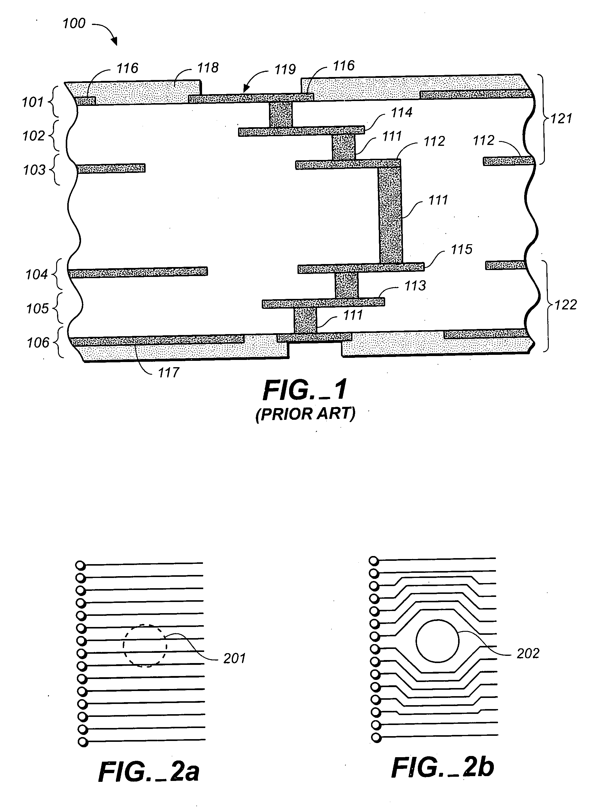
This causes considerable trace crowding and can lead to cross talk between the traces.
Also, the close proximity of the traces to the via itself can induce many undesirable effects.
This is particularly time consuming, especially with respect to the redesign of the signal planes which involve a great deal of expensive engineering time in order to achieve.
This type of redesign results in greater cross talk between adjacent signal traces and requires redesign of all layers of the package design.
Presently there are no satisfactory processes for converting packages designed for use without decoupling capacitors into packages for use with decoupling capacitors.

Method used


Image

  • Package configuration and manufacturing method enabling the addition of decoupling capacitors to standard package designs
  • Package configuration and manufacturing method enabling the addition of decoupling capacitors to standard package designs
  • Package configuration and manufacturing method enabling the addition of decoupling capacitors to standard package designs

Examples


Embodiment Construction

[0023] The present invention has been particularly shown and described with respect to certain embodiments and specific features thereof. The embodiments set forth hereinbelow are to be taken as illustrative rather than limiting. It should be readily apparent to those of ordinary skill in the art that various changes and modifications in form and detail may be made without departing from the spirit and scope of the invention.

[0024] In the following detailed description, various integrated circuit packages and method embodiments for constructing such packages will be disclosed.

[0025] The inventors, as well as others, have noted that it is very difficult to convert integrated circuit package designs conceived for use without decoupling capacitors into packages capable of implementing decoupling capacitors. The inventors have created a low cost method of constructing such packages using prior designs. The inventors approach is extremely efficient because it does not entail the wholes...


PUM


Abstract

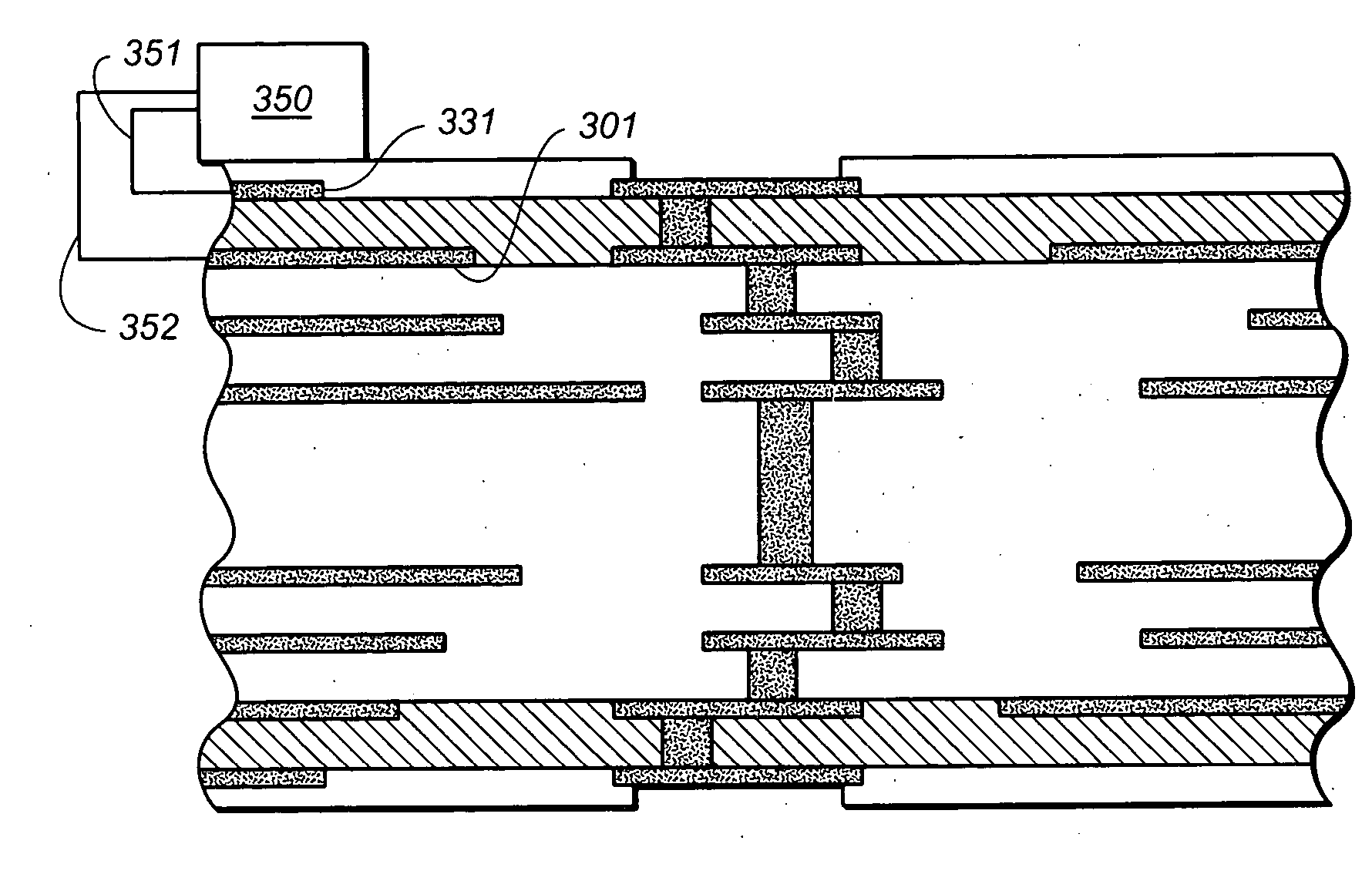
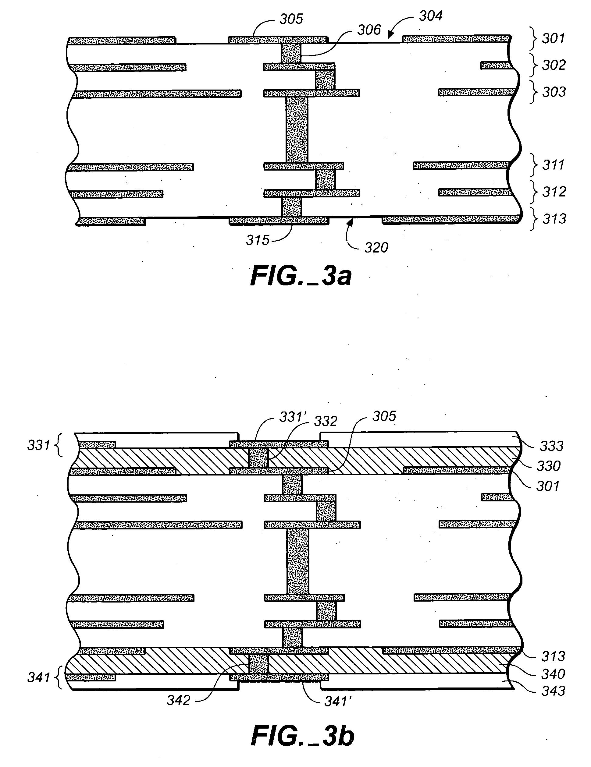
The present invention is directed to a method of fabricating an integrated circuit package having decoupling capacitors using a package design conceived for use without decoupling capacitors. The package is implemented with a minimal redesign of the original design and not requiring any redesign of the signal trace pattern. The invention involves replacing top and bottom bond pads with via straps and then covering the top and bottom reference planes with a dielectric layer having conductive vias that electrically connect with the underlying via straps. Planes having the opposite polarity of the underlying reference plane are then formed on the dielectric layer. These planes include an array of bonding pads in registry with the vias. Decoupling capacitors are mounted to the top of the package and electrically connected with the plane on top of the package and the immediately underlying reference plane without the electrical connections to the capacitors passing through the signal planes of the package.

Description

FIELD OF THE INVENTION [0001] The invention described herein relates generally to semiconductor device packages and the methods of their construction. In particular, the present invention relates to methods and structures used to adapt package designs originally configured for use without decoupling capacitors. More particularly, some embodiments of the invention adapt such package designs in a manner that the addition of decoupling capacitors does not require significant re-routing of electrical traces formed at the signal layers of the package. BACKGROUND OF THE INVENTION [0002] Decoupling capacitors are usually placed on integrated circuit (IC) packages between external power sources and the delicate circuitry contained in the package. Commonly, such decoupling capacitors are used to buffer the circuitry of the package from power fluctuations common in the external sources. Such fluctuations can be fatal to delicate or less robustly designed circuitry of the package. Decoupling c...

Claims


Application Information

Patent Timeline
Patent Type & Authority Applications(United States)
IPC IPC(8): H01L29/00
CPCH01L23/49822H01L23/49838H01L23/50H05K1/0231H05K1/112H05K1/162H05K3/4644H05K3/4688H05K2201/09309H01L2924/0002H01L2924/00
Inventor MILLER, LEAHBARBER, IVORTHURAIRAJARATNAM, ARITHARAN
Owner BELL SEMICON LLC
Learn More