
Dual work function CMOS gate technology based on metal interdiffusion

a metal interdiffusion and dual work technology, applied in the field of cmos semiconductor transistors and circuits, can solve the problems of polycrystalline silicon not being the best choice for this application, overcoming limitations, unstable polycrystalline silicon, etc., and achieves the effect of effective altering the gate work function of the second metal gate, favorable threshold voltage, and high diffusivity

Inactive Publication Date: 2006-11-28
RGT UNIV OF CALIFORNIA
View PDF9 Cites 21 Cited by
  • Summary
  • Abstract
  • Description
  • Claims
  • Application Information

AI Technical Summary

Benefits of technology

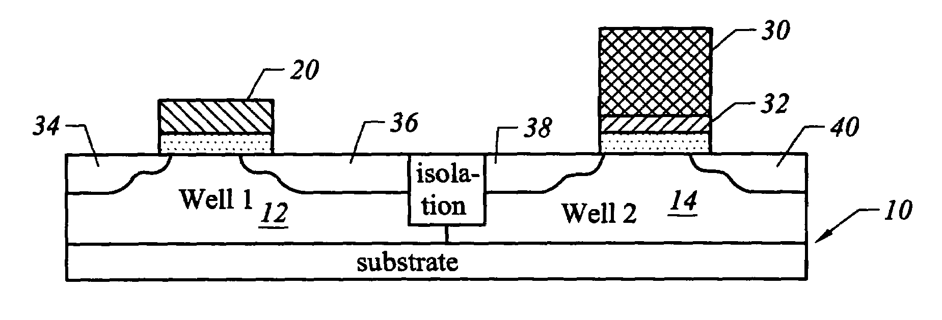
[0008]In one embodiment, two layers of different metals are formed on gate dielectric overlying P and N wells in a semiconductor substrate. The top or second layer of metal is removed from over one well, and then the metal layers are annealed at an elevated temperature. The bottom or first layer of metal forms a first metal gate, and the metal from the top or second layer diffuses through the bottom or first layer and effectively alters the gate work function of the second metal gate.
[0009]In order to fabricate bulk p- and n-MOS devices with favorable threshold voltages, one of the metals must have a work function similar to that of n-type silicon (for example, Ti, Ta, Nb), and the other metal must have a work function similar to that of P-type silicon (for example, Ni, Ir, Mo). It is also important that the second metal (top layer metal) has a sufficiently high diffusivity in the first metal (bottom layer metal) and has a propensity to segregate to the gate dielectric interface. A good example of such a pair of metals is Ni and Ti. Ni diffuses easily through Ti and segregates at the silicon oxide interface.
[0010]In other embodiments, a barrier layer can be provided between the first and second metal layers over the doped well where no metal diffusion is desired. This is done before the second or top metal layer is formed by first forming the barrier layer over both wells and then selectively removing the barrier layer where metal diffusion is desired. Alternatively, the barrier layer can be left in place over both wells, and after the second metal layer is formed over the barrier layer, the barrier can be effectively removed from over one well by selective ion implant into the barrier layer.
[0011]The metal diffusion process is readily employed either before or after source and drain formation, thereby avoiding high temperature processing in forming the source and drain regions, if necessary.

Problems solved by technology

As device scaling continues beyond the 100 nm technology node, polycrystalline silicon might no longer remain the best choice for this application.
Metal gate electrodes overcome these limitations, due to high free electron concentration in the metallic materials.
Polycrystalline silicon is also unstable on the many advanced (high permittivity) gate dielectrics.
In addition, metal gate materials may ultimately be necessary for high-k gate dielectrics because polycrystalline silicon has been found to be thermodynamically unstable on some high-k materials such as Ta2O5 and ZrO2.
Unfortunately, this approach exposes the gate dielectric to a metal-etching process in the regions from which the first gate metal is selectively removed, and consequently causes undesirable thinning of the gate dielectric and potential reliability problems.

Method used


Image

  • Dual work function CMOS gate technology based on metal interdiffusion
  • Dual work function CMOS gate technology based on metal interdiffusion
  • Dual work function CMOS gate technology based on metal interdiffusion

Examples


Embodiment Construction

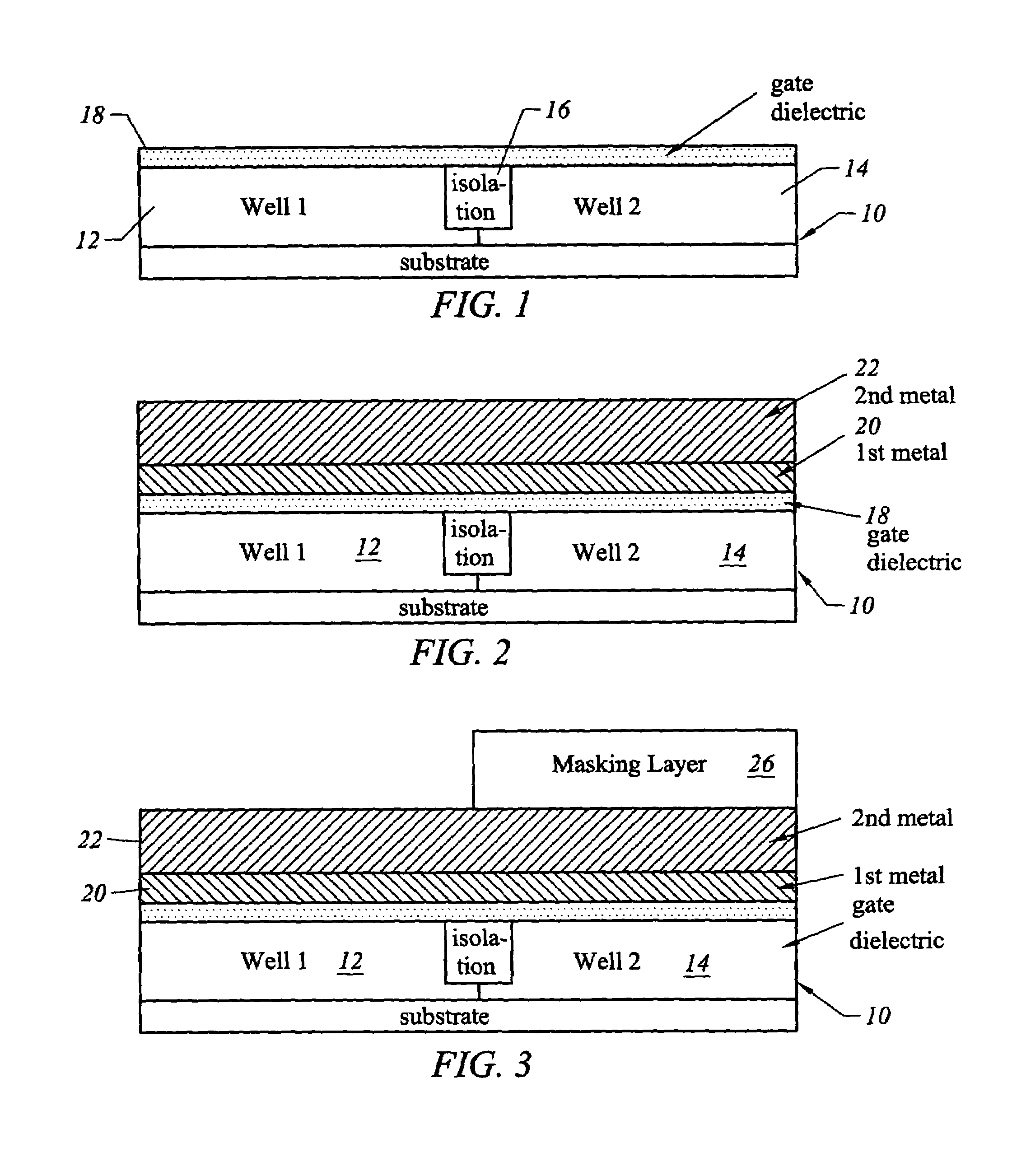
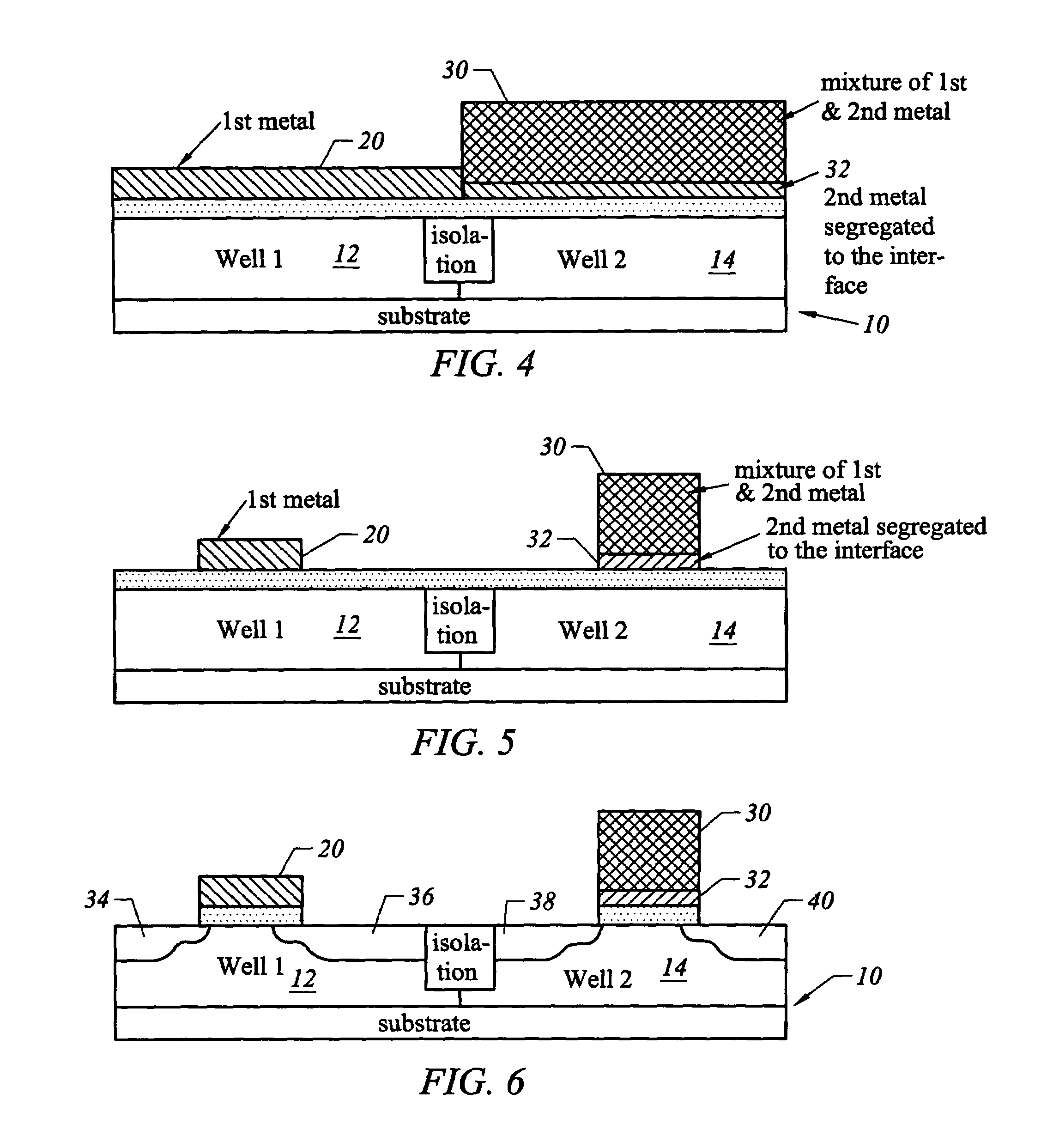
[0021]FIGS. 1–6 are section views illustrating the fabrication of a CMOS pair in accordance with one embodiment of the invention. In this embodiment, titanium, Ti, is employed as a first metal layer, and nickel, Ni, is employed as the second metal layer since Ni diffuses easily through Ti and segregates at the silicon oxide interface. Moreover, Ti has a work function similar to that of n-type silicon, whereas Ni has a work function similar to that of p-type silicon.

[0022]In FIG. 1 a silicon substrate 10 has a p-doped well 1 shown at 12 and an n-doped well 2 shown at 14 formed in a surface of the substrate with an isolation region 16 separating the two wells. A gate dielectric 18 of silicon oxide, for example, is formed on the surface of the two wells.

[0023]In FIG. 2 a first metal layer 20 of titanium is formed on silicon oxide layer 18, and a second metal layer 22 of nickel is formed over the titanium layer 20. The two metal layers are preferably formed by chemical vapor deposition ...


PUM

PropertyMeasurementUnit
work functionaaaaaaaaaa
thicknessaaaaaaaaaa

Abstract

A gate structure for a MOSFET device comprises a gate insulation layer, a first layer of a first metal abutting the gate insulation layer, and a second layer overlying the first layer and comprising a mixture of the metal of the first layer and a second metal, the metal layers formed by the diffusion of the first metal into and through the second metal. The second metal can be used as the gate for a n-MOS transistor, and the mixture of first metal and second metal overlying a layer of the first metal can be used as a gate for a p-MOS transistor where the first metal has a work function of about 5.2 eV and the second metal has a work function of about 4.1 eV.

Description

CROSS-REFERENCES TO RELATED APPLICATIONS[0001]This application is a divisional of application Ser. No. 10 / 315,476, now U.S. Pat. No. 6,794,234, filed Dec. 9, 2002, from which priority under 35 U.S.C. §120 is claimed, and which is incorporated herein by reference. Parent patent application Ser. No. 10 / 315,476 claims priority from Provisional Patent Application No. 60 / 353,786, filed Jan. 30, 2002, which is incorporated herein by reference.BACKGROUND OF THE INVENTION[0002]This invention relates generally to CMOS semiconductor transistors and circuits, and more particularly the invention relates to CMOS transistors having dual work function metal gates and methods of manufacturing the same.[0003]In producing high performance bulk CMOS integrated circuits, both n-MOS and pMOS transistors must have low threshold voltages (VT). This in turn requires that the gate electrodes for the n-MOS and p-MOS transistors have different work functions. The desired work function for n-MOS transistors is...

Claims


Application Information

Patent Timeline
Patent Type & Authority Patents(United States)
IPC IPC(8): H01L29/49H01L21/28H01L21/8238
CPCH01L21/28079H01L21/823842H01L29/4958
Inventor POLISHCHUK, IGORRANADE, PUSHKARKING, TSU-JAEHU, CHENMING
Owner RGT UNIV OF CALIFORNIA
Learn More