High-temperature superconducting device and manufacturing method thereof
a superconducting device and manufacturing method technology, applied in the direction of superconductor devices, semiconductor devices, electrical devices, etc., can solve the problems of no longer being fulfilled, circuits cannot be operated, and generating parasitic inductance, etc., to achieve stable high-speed operation
- Summary
- Abstract
- Description
- Claims
- Application Information
AI Technical Summary
Benefits of technology
Problems solved by technology
Method used
Image
Examples
first embodiment
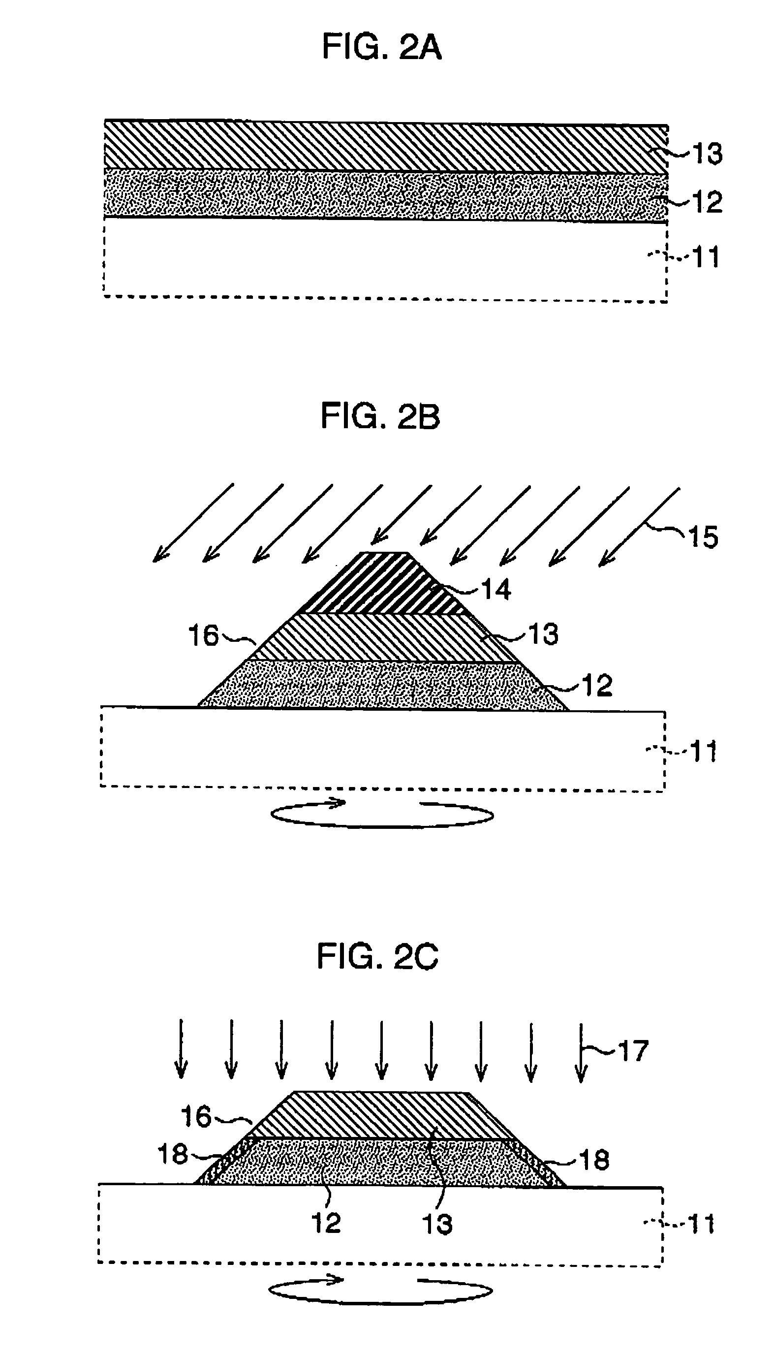
[0060]Hereinafter, a forming process of an interface-engineered ramp-edge junction according to the present invention is explained with reference to FIGS. 2A to 4B.
[0061]First, as shown in 2A, a laser deposition method (PLD: pulse laser deposition) is used to sequentially deposit a lower electrode layer 12 formed of YBCO (YBa2Cu3O7-x) having a thickness of 200 nm for example, and an insulating layer 13 formed of a LSAT having a thickness of 300 nm for example, on a LSAT substrate 11 formed of [LaAlO3]0.3[Sr(Al,Ta)O3]0.7.
[0062]Next, as shown in 2B, a photo-resist is coated on the insulating layer 13, which is then exposed and developed. After that, the photo-resist film is reflowed by baking, so that a photo-resist pattern 14 is formed. The photo-resist pattern 14 is then used as a mask, so as to irradiate argon ion 15 from a diagonal direction with the LSAT substrate 11 rotated such that the insulating layer 13 and the lower electrode layer 12 are etched, resulting in formation of a...
second embodiment
[0068]Next, with reference to FIGS. 5A to 6B, a forming process of an interface-engineered ramp-edge junction according to the present invention will be explained.
[0069]First, as shown in FIG. 5A, as with the above-described first embodiment, a laser deposition method is used to sequentially deposit on a LSAT substrate a lower electrode layer 12 formed of YBCO (YBa2Cu3O7-x) having a thickness of 200 nm for example, and an insulating layer 13 formed of LSAT having a thickness of 300 nm for example.
[0070]Subsequently, a photo-resist is coated on the insulating layer 13, which is then exposed and developed. The photo-resist film is then reflowed by baking, so that a photo-resist pattern 14 is formed. The photo-resist pattern 14 is then used as a mask, so as to irradiate argon ion 15 from a diagonal direction with the LSAT substrate 11 rotated, such that the insulating layer 13 and the lower electrode layer 12 are etched, resulting in formation of a ramp slope 16.
[0071]As shown in FIG. ...
third embodiment
[0075]With the above-described conditions as premises, a superconducting circuit device according to the present invention will be explained next.
[0076]FIG. 7 shows an equivalent circuit diagram of a DC / SFQ conversion circuit, which is one example of a pulse generating circuit, the pulse generating circuit being a basis of the superconducting circuit device in the third embodiment of the present invention.
[0077]The circuit applies normal electrical signal used in semiconductor circuits through an input Isgn, and an SFQ pulse is outputted from an output terminal when an input signal exceeds a certain threshold level, where, the larger is the product of Ic×Rn of a Josephson junction used in the circuit, the narrower the time width of the generated pulse becomes. This state will be explained with reference to FIG. 8.
[0078]FIG. 8 shows simulation results of generated pulses where the product of Ic×Rn is set to 0.5 mV, 1.0 mV, and 1.5 mV.
[0079]The half widths of the pulses are 5.8 ps (pi...
PUM
 Abstract
Description
Claims
Application Information
 - R&D
- Intellectual Property
- Life Sciences
- Materials
- Tech Scout
- Unparalleled Data Quality
- Higher Quality Content
- 60% Fewer Hallucinations
Browse by: Latest US Patents, China's latest patents, Technical Efficacy Thesaurus, Application Domain, Technology Topic, Popular Technical Reports.
© 2025 PatSnap. All rights reserved.Legal|Privacy policy|Modern Slavery Act Transparency Statement|Sitemap|About US| Contact US: help@patsnap.com


