Method of manufacturing mask for electron beam lithography and mask blank for electron beam lithography

Inactive Publication Date: 2006-04-18
TOKYO ELECTRON LTD
View PDF6 Cites 2 Cited by
  • Summary
  • Abstract
  • Description
  • Claims
  • Application Information

AI Technical Summary

Benefits of technology

[0032]Accordingly, the protective layer and the hard mask can be formed easily at once, manufacture performance and productivity can be enhanced, and manufacture facilities can be utilized efficiently.
[0036]Filling the filling material into the space portion could prevent the space portion from causing problems during an etching process or the like. That is, no deformation or damage is caused to the SOI layer when the side of the silicon base layer of the SOI substrate is stuck to a vacuum chuck for forming a resist film on the SOI layer by spin-coating or the like. No loss of electrostatic attraction force in relation to the depth of the space portion (distance from a surface of the vacuum chuck) is caused when the side of the silicon base layer of the SOI substrate is stuck to an electrostatic chuck for etching the SOI layer. No irregular electrical discharge would be caused when the SOI layer is etched. Furthermore, the silicon base layer can be etched in a uniform temperature since an even flow of cooling gas from a susceptor can be achieved.
[0039]Thus structured, the mask blank can prevent a chuck or the like from damaging the front side of the SOI layer, for example, when the silicon base layer is processed. Therefore, the SOI layer can be patterned with no defect. Furthermore, the mask blank enables a resist mask to be formed on a back side of a silicon base layer without any complicated procedure, and also prevents problems caused by resist residue (scum) remaining thereto.
[0041]Accordingly, the front side of the SOI layer and the back side of the silicon base layer can be protected from damage when handling (e.g. transporting, storing) the mask blank as an intermediary product.
[0044]Therefore, other than obtaining the same benefits as those of the aforementioned mask blank formed with the protective layer and the hard mask, this mask blank can also prevent the space portion from causing problems during an etching process or the like.

Problems solved by technology

Therefore, the conventional method of manufacturing a lithographic mask risks damaging the front side of the SOI layer when conveying or processing the SOI substrate, and may not be able to form a desired pattern.
Furthermore, in a case where the silicon base layer has a considerable thickness, forming a resist film with a typical thickness of a few micrometers would not be enough to prevent etching damage.
Forming the resist film with such thickness is however inconvenient and causes complication in a coating process since the coating procedure is required to be performed repetitively for numerous times. Forming the resist film with such thickness could also cause difficulty in thoroughly removing etching residue in a cleaning process subsequent to an ashing process.
Fixing the SOI substrate in such manner however could cause a problem such as deformation or damage to the SOI layer owing to the presence of a space portion (aperture) 6 shown in FIG. 7C.

Method used


Image

  • Method of manufacturing mask for electron beam lithography and mask blank for electron beam lithography
  • Method of manufacturing mask for electron beam lithography and mask blank for electron beam lithography
  • Method of manufacturing mask for electron beam lithography and mask blank for electron beam lithography

Examples


Embodiment Construction

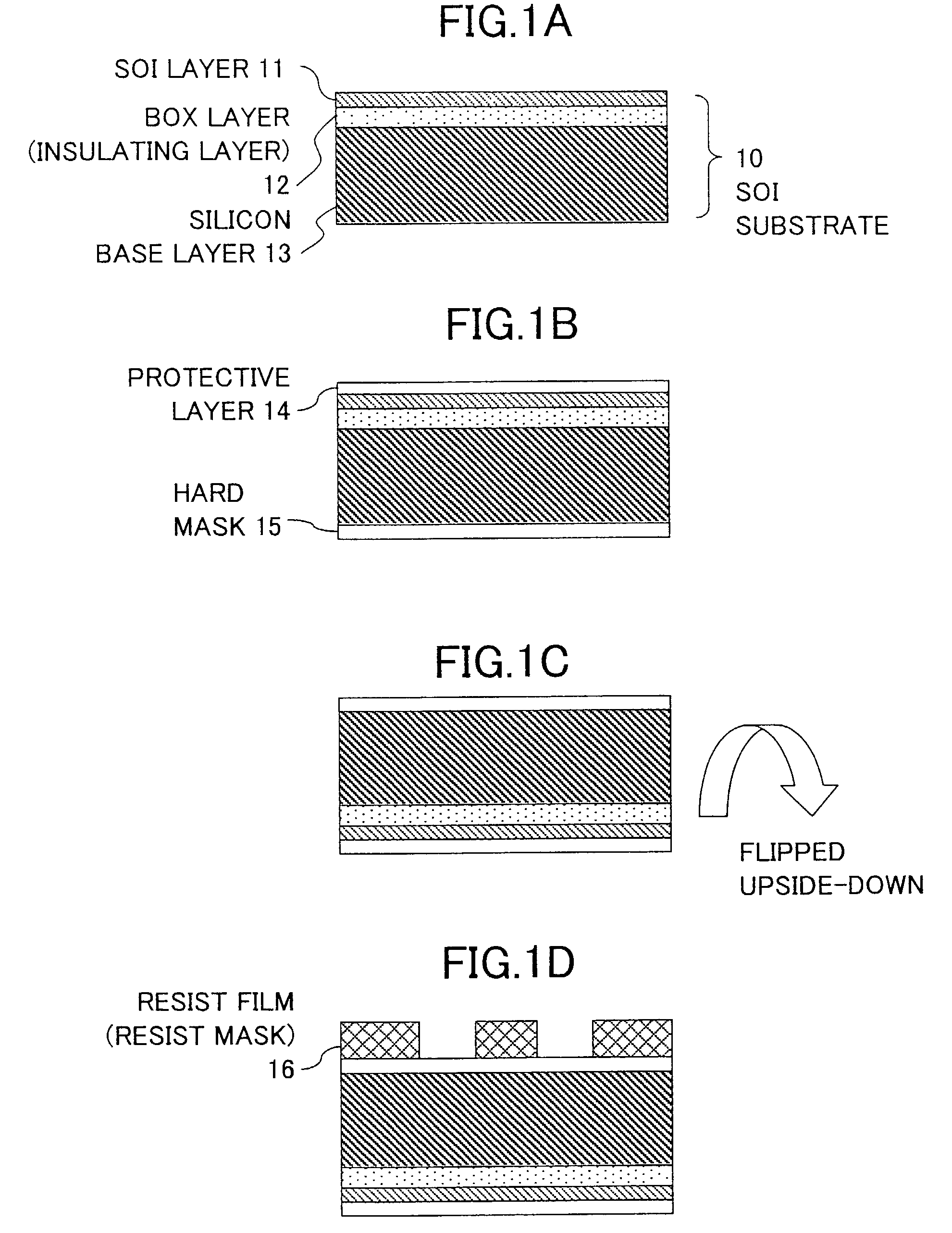
[0055]In the following, embodiments of the present invention regarding a method for manufacturing a mask for electron beam lithography and a mask blank for electron beam lithography will be described with reference to the accompanying drawings.

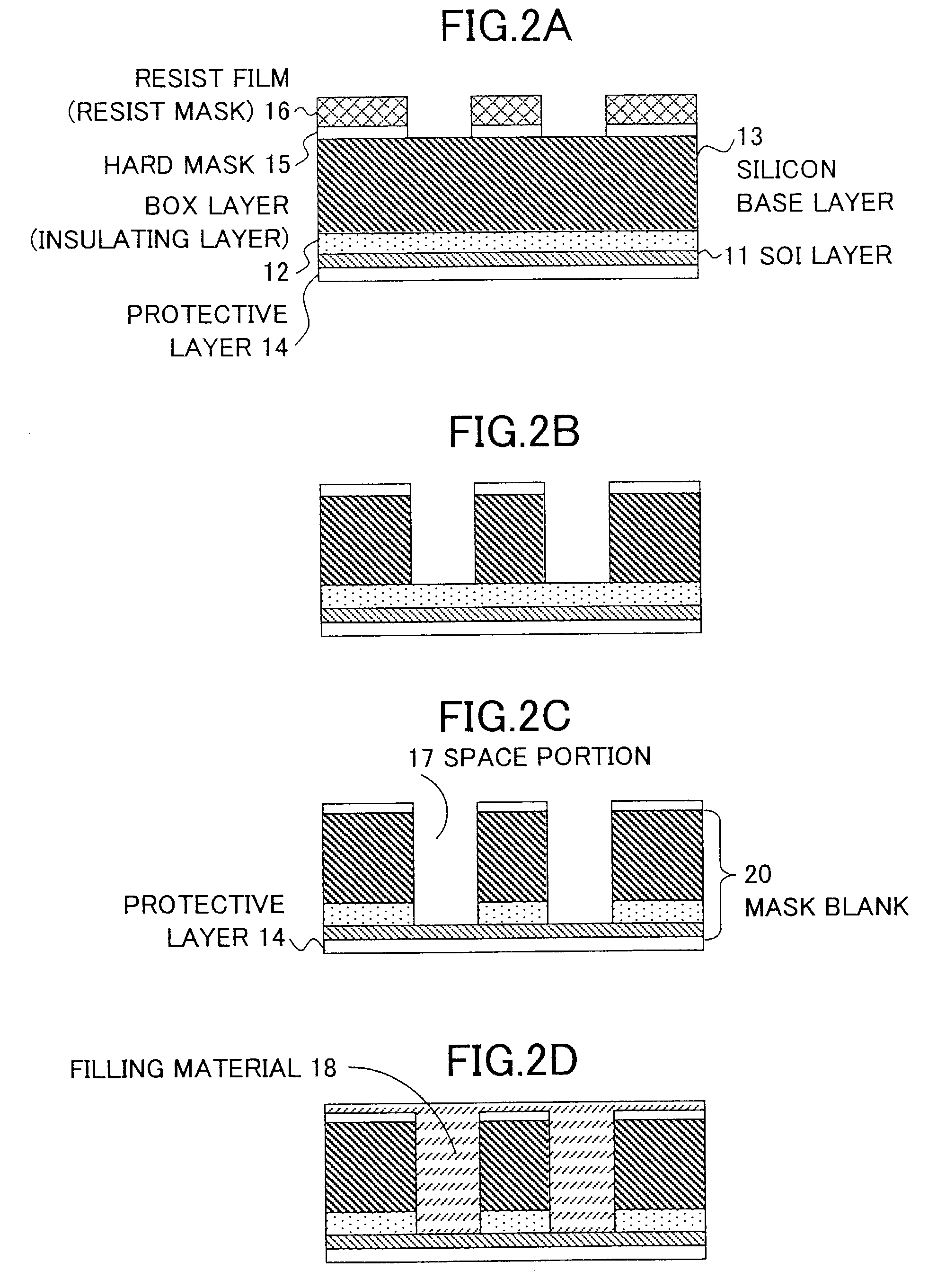
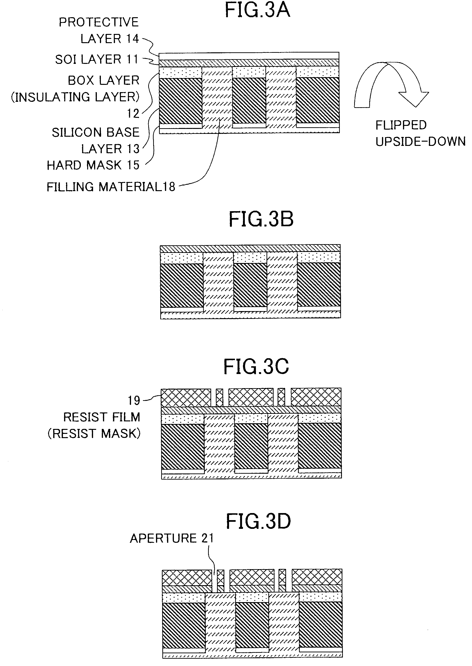
[0056]An embodiment regarding a method for manufacturing a mask for electron beam lithography will be described with reference to FIG. 1A to FIG. 4B.

[0057]First, an SOI substrate 10 is prepared as a material for manufacturing a mask for electron beam lithography (hereinafter simply referred as “lithographic mask”). The SOI substrate 10 has, for example, a silicon base layer 13 with a thickness of approximately 600 micrometers, a BOX layer 12 (Buried Oxide Layer) arranged above the silicon base layer 13 for serving as an SiO2 insulating layer with a thickness of approximately few micrometers, and an SOI layer 11 arranged above the BOX layer 12 with a thickness of approximately few micrometers (See FIG. 1A).

[0058]After the SOI substrate 10 is th...


PUM


Abstract

This invention provides a method of manufacturing mask for electron beam lithography and a mask blank for electron beam lithography, which could prevent damage upon a front side of an SOI (Silicon On Insulator) layer and also provide desirable etching of a silicon base layer of an SOI substrate is used.A mask blank for electron beam lithography is manufactured as an intermediary product by etching a silicon base layer and a BOX layer subsequent to forming a protective layer on a front side of an SOI (Silicon On Insulator) layer simultaneously with forming a hard mask on a back side of the SOI layer. Then, an etching process is performed upon the SOI layer to thereby complete a manufacture process of a mask for electron beam lithography having an aperture for transmitting an electron beam therethrough.

Description

BACKGROUND OF THE INVENTION[0001]1. Field of the Invention[0002]The present invention generally relates to a method for manufacturing a mask for electron beam lithography and a mask blank for electron beam lithography.[0003]2. Description of the Related Art[0004]In general, a semiconductor integrated circuit or the like is formed by repetitively performing a variety of processes (e.g. deposition, oxidation, diffusion, etching) upon a semiconductor wafer.[0005]Owing to today's very large scale integration of the semiconductor device, there is a need to form, for example, oxidized layers, or metal wires on a semiconductor wafer in submicroscopic sizes.[0006]Therefore, a lithographic technique for forming sub-microscopic patterns, and an etching technique for anisotropically etching a resist film having a sub-microscopic pattern formed thereto are indispensable in fulfilling such need.[0007]RIE (Reactive Ion Etching) providing highly anisotropic etching is one preferable example of the...

Claims


Application Information

Patent Timeline
IPC IPC(8): G03F9/00G03C5/00G03F1/20G03F1/48H01L21/027
CPCG03F1/20Y10S430/143
Inventor YUASA, MITSUHIRO
Owner TOKYO ELECTRON LTD
Why Eureka
Try Eureka