Semiconductor device, layout design method thereof, and layout design device using the same

a technology of semiconductor devices and layouts, applied in the field of semiconductor devices, can solve problems such as inability to ensure flatness, and achieve the effects of avoiding electrostatic connection, ensuring the flatness of semiconductor devices, and avoiding involuntary formation of conductive channels

Inactive Publication Date: 2010-03-16
COLUMBIA PEAK VENTURES LLC
View PDF15 Cites 0 Cited by
  • Summary
  • Abstract
  • Description
  • Claims
  • Application Information

AI Technical Summary

Benefits of technology

[0009]An advantage of the invention is to provide a semiconductor device with a layout that avoids causing problems to internal circuits, a method for designing a layout of such semiconductor device, and a layout design device that uses the method, where the problems are caused by an involuntarily formed conductive channel created by dummy activation areas and dummy wirings which are provided in order to ensure the flatness of the semiconductor device.
[0010]According to a first aspect of the invention, a semiconductor device that has a multilayer structure includes, in each layer, a dummy pattern for ensuring a flatness thereof; a pad area in which a bonding pad is formed; an input-output circuit area in which an input-output circuit is formed, the input-output circuit area being adjacent to the pad area in plan view; and a dummy pattern confined area for forbidding an arrangement of the dummy pattern in every layer included in the semiconductor device, the dummy pattern confined area being provided between the pad area and the input-output circuit area in plan view.
[0011]This allows avoiding the involuntary formation of conductive channel through bonding pads and through dummy patterns, as well as avoiding the electrostatic connection within the internal circuit through the conductive channel.
[0012]In this case, the dummy pattern confined area is provided between the pad area and the input-output circuit area adjacent thereto, only if a distance therebetween is equal to or less than a defined value set in advance. Here, the defined value is set to produce a distance which allows ensuring the flatness.
[0013]With this structure, the dummy pattern is provided if the above distance is larger than the determined value. Therefore, the flatness is ensured, since the dummy pattern is set when the distance between the pad area and the input-output circuit is relatively long, and is predicted that the flatness cannot be ensured.
[0014]In this case, the dummy pattern serves as a dummy wiring, and the bonding pad and the input-output circuit constitute a circuit having a multilayer pad structure. Here, every layer thereof is lower than the bonding pad, and includes a conductor arranged on the entire surface of the pad area in plan view. Moreover, the dummy pattern confined area is provided, in plan view, to the pad area, to the input-output circuit area, and to a power separation circuit area in which a power separation circuit for separating a power system is formed.

Problems solved by technology

These cases, however, may involve occurrences of phenomenon where static electricity is transmitted to internal circuits.
Therefore, the flatness is ensured, since the dummy pattern is set when the distance between the pad area and the input-output circuit is relatively long, and is predicted that the flatness cannot be ensured.

Method used


Image

  • Semiconductor device, layout design method thereof, and layout design device using the same
  • Semiconductor device, layout design method thereof, and layout design device using the same
  • Semiconductor device, layout design method thereof, and layout design device using the same

Examples


Embodiment Construction

[0034]An embodiment of the present invention will now be described.

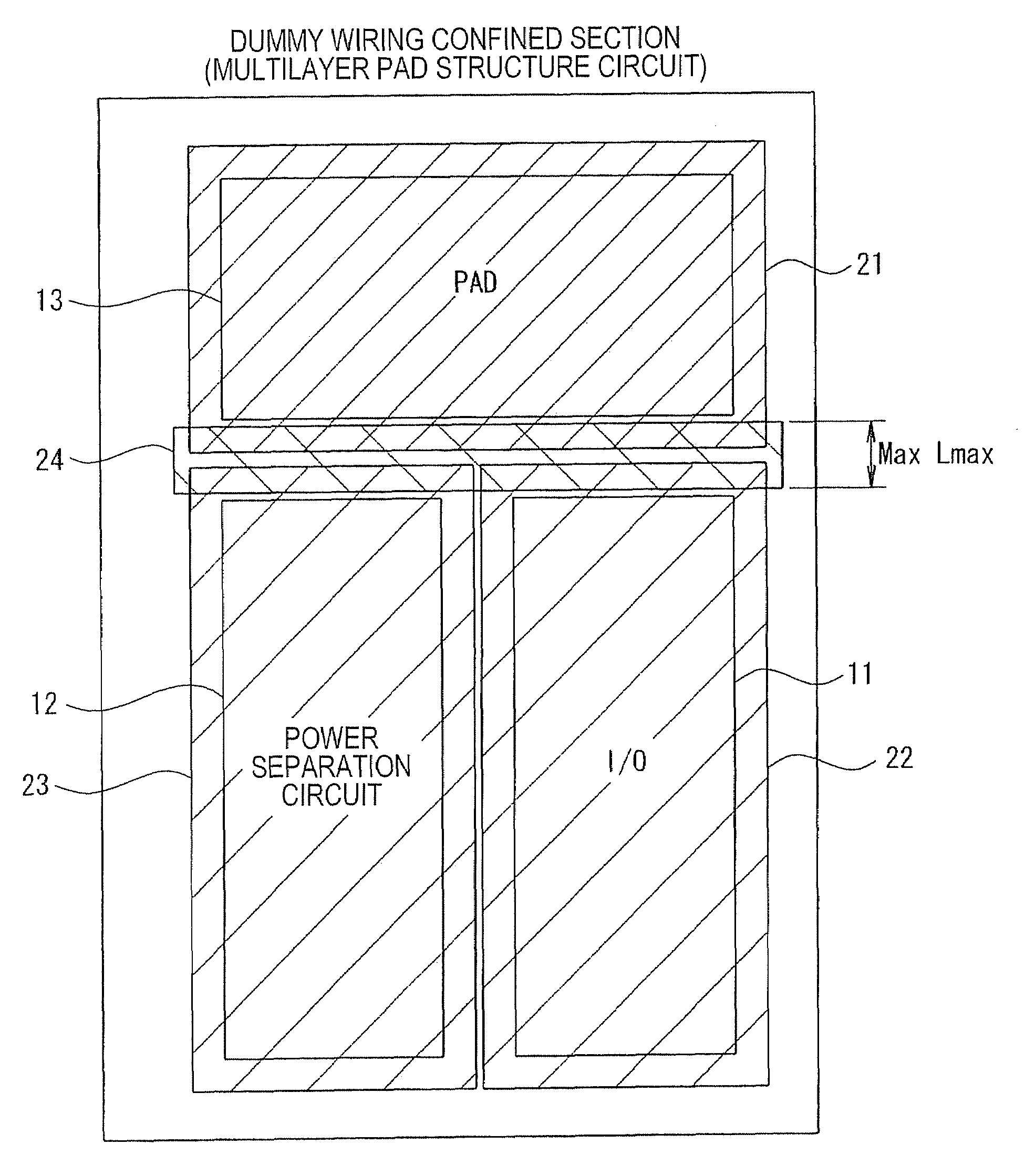
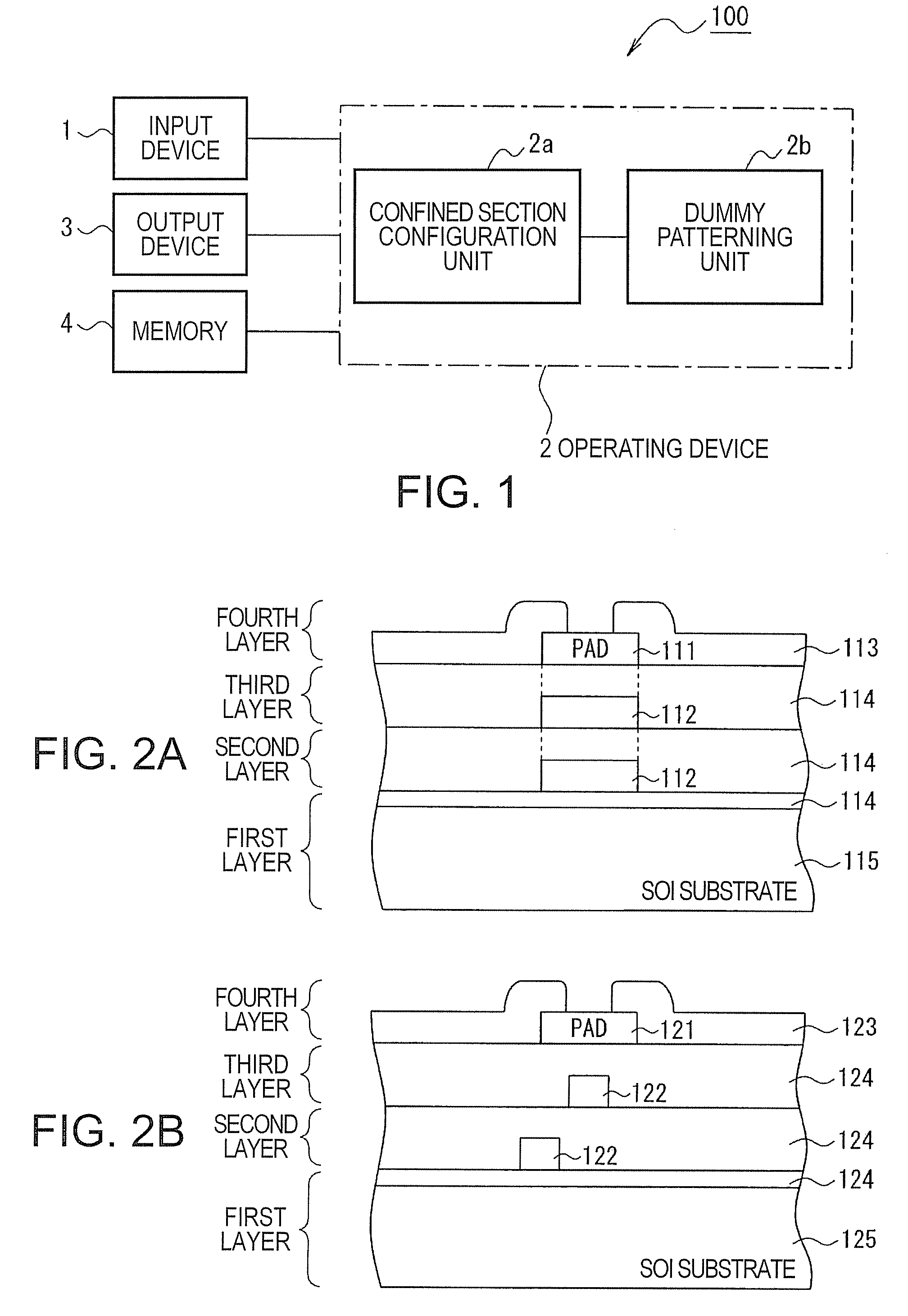
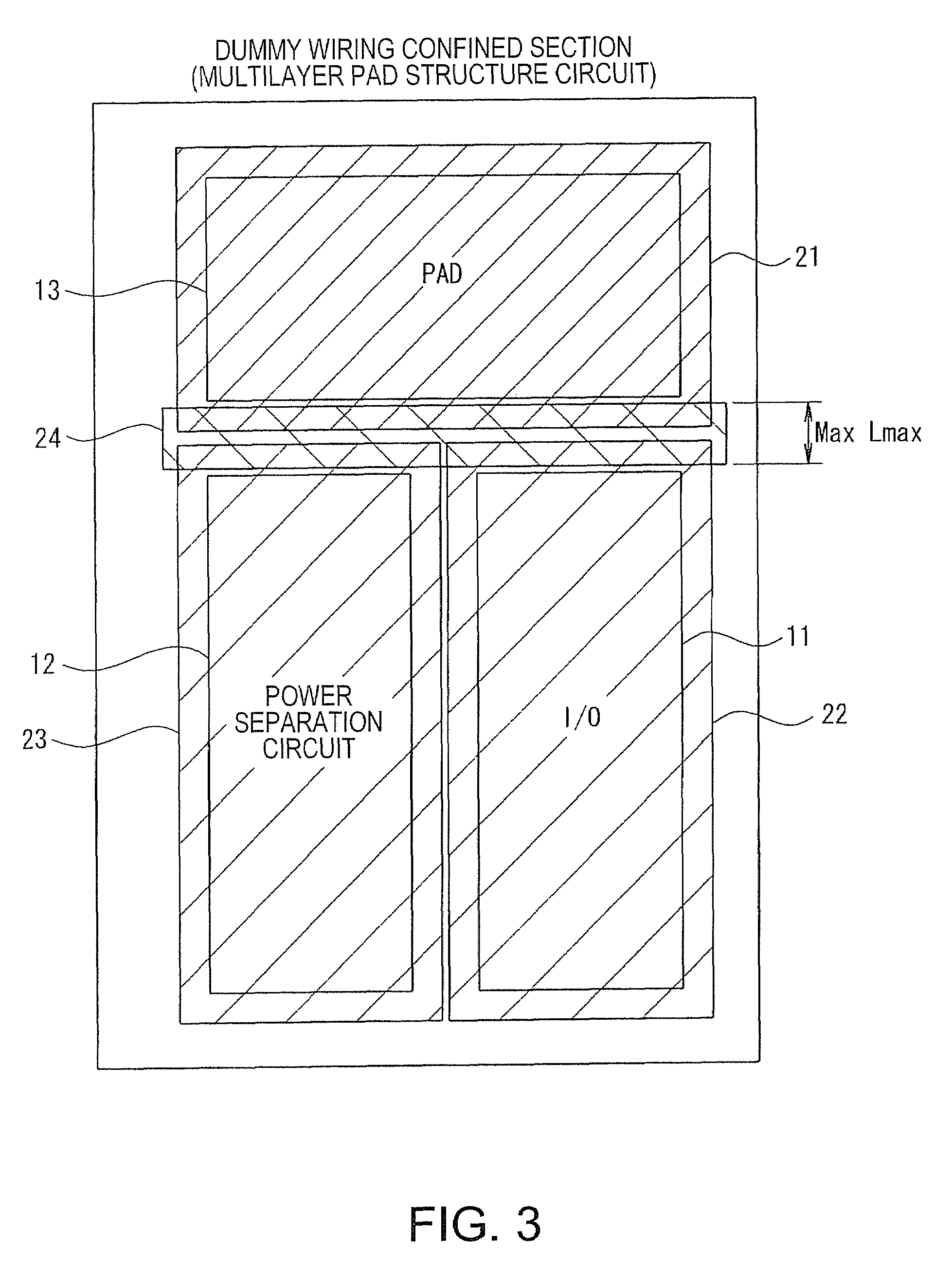
[0035]FIG. 1 is an example of a layout design device 100 to which aspects of the invention are applied. This layout design device 100 includes an input device 1, an operating device 2, an output device 3, and a memory unit 4 for storing various sets of information. The input device 1 includes a keyboard and an interface for inputting CAD product data which contains the placement information of components constituting a semiconductor device for designing the layout thereof. Examples of components include a bonding pad (hereafter referred to as a pad), an input-output circuit, an internal circuit thereof, and a wiring coupling the aforementioned components. The operating device 2 sets, based on the product CAD data input thereto, dummy pattern confined sections (dummy pattern confined areas) for assigning areas to forbid patterning dummy activation areas and dummy wirings (i.e. dummy patterns) used for planarizing a se...


PUM


Abstract

A semiconductor device having a multilayer structure, each layer including: a dummy pattern for ensuring a flatness thereof; a pad area in which a bonding pad is formed; an input-output circuit area in which an input-output circuit is formed, the input-output circuit area being adjacent to the pad area in plan view; and a dummy pattern confined area for forbidding an arrangement of the dummy pattern in every layer included in the semiconductor device, the dummy pattern confined area being provided between the pad area and the input-output circuit area in plan view.

Description

[0001]The entire disclosure of Japanese Patent Application No. 2006-331915, filed Dec. 8, 2006 is expressly incorporated by reference herein.BACKGROUND[0002]1. Technical Field[0003]The present invention relates to a semiconductor device fabricated using a chemical-mechanical polishing (CMP) method, the semiconductor device being provided with shallow trench isolation (STI) and wire structures. The present invention also relates to a layout design method of such semiconductor device and a layout design device that uses the method.[0004]2. Related Art[0005]Commonly introduced elements and wiring structures of semiconductor devices have thin-film multilayer structures, in order to make semiconductor devices more highly integrated and greatly reduced in scale. The manufacturing of these elements involves a CMP method for planarizing deposited surfaces, and the flatness of the substrate polished by this method depends on the layout of the wirings. In order to ensure the flatness, a sugge...

Claims


Application Information

Patent Timeline
Patent Type & Authority Patents(United States)
IPC IPC(8): H01L23/50
CPCG06F17/5068H01L23/522H01L23/585H01L23/62H01L24/02G06F30/39H01L24/05
Inventor KATO, YOSHIHIKO
Owner COLUMBIA PEAK VENTURES LLC
Why Eureka
Try Eureka