Low temperature nitride used as Cu barrier layer
- Summary
- Abstract
- Description
- Claims
- Application Information
AI Technical Summary
Benefits of technology
Problems solved by technology
Method used
Image
Examples
Embodiment Construction
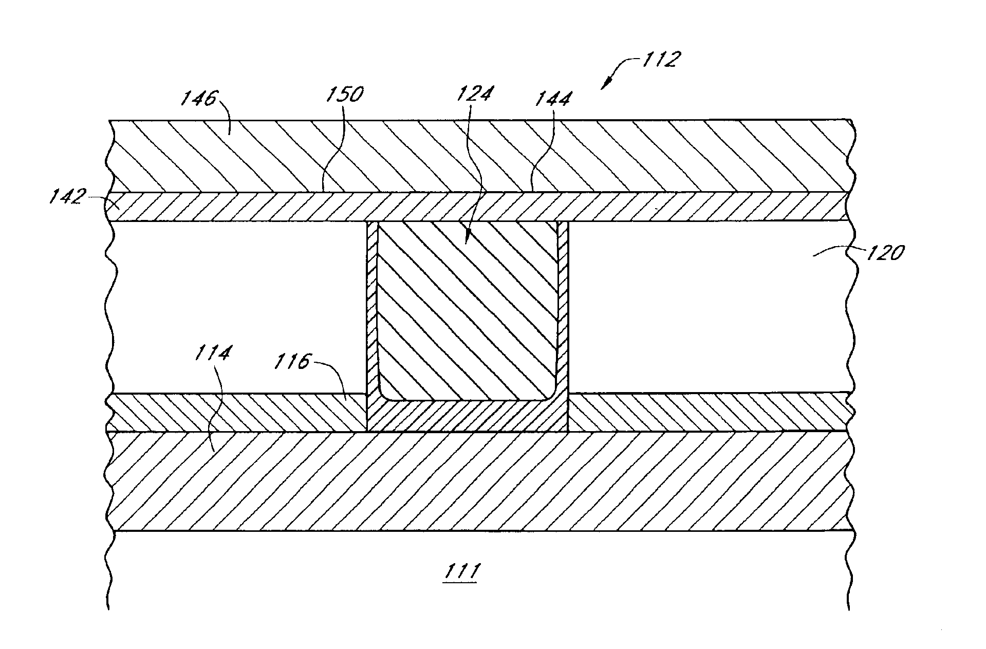
[0026]Reference will now be made to the drawings wherein like numerals refer to like parts throughout. As will be described herein below, the process of the preferred embodiment provides a method of depositing a non-conductive barrier layer onto a copper surface wherein the barrier layer comprises a nitride film.
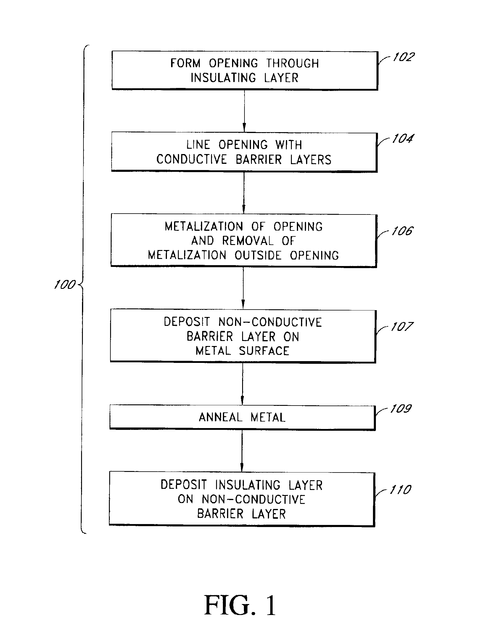
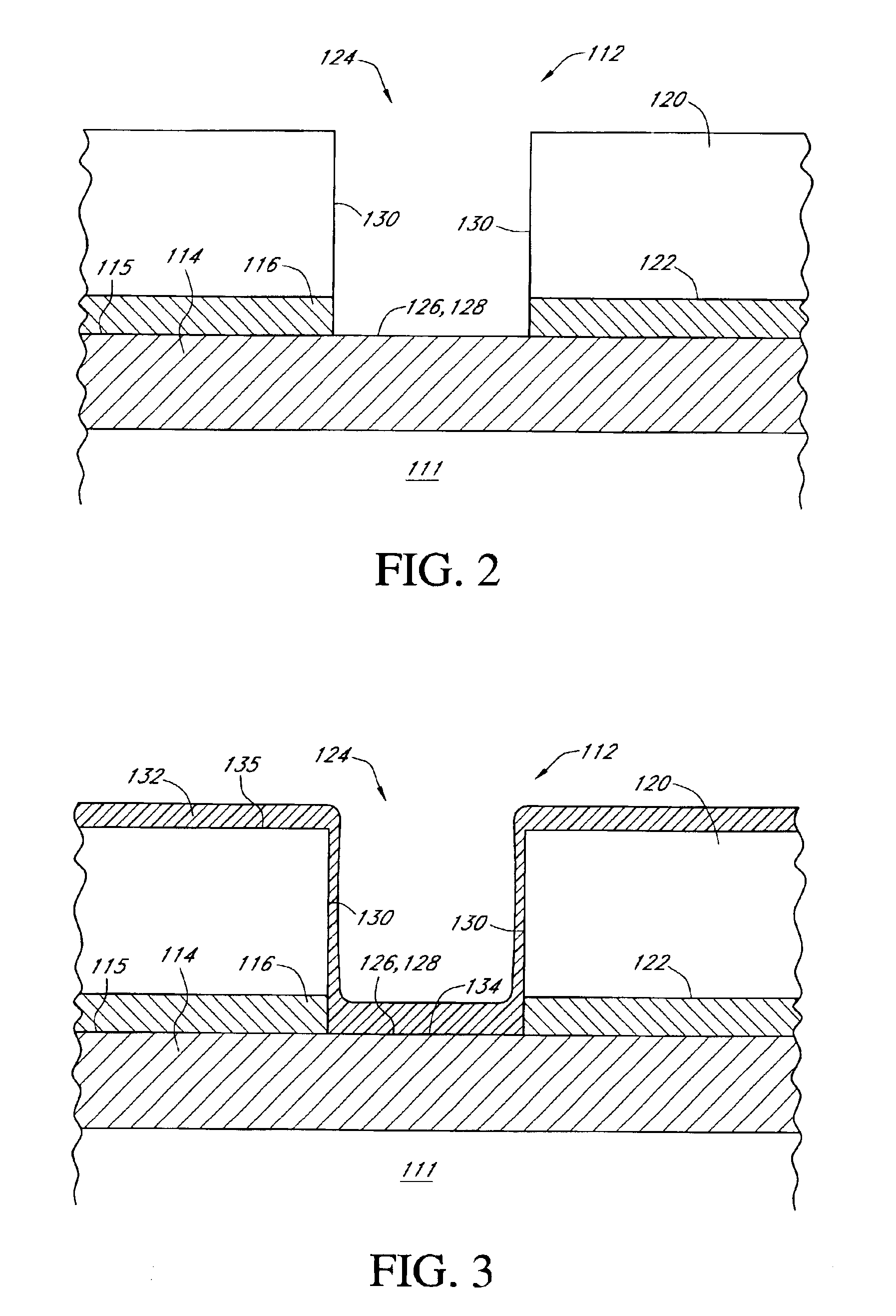
[0027]FIG. 1 schematically illustrates a process flow 100 of the preferred embodiment of forming a non-conductive barrier film between a top surface of a conductive layer and a bottom surface of an insulating layer. As shown in FIG. 1, the process begins with a first step 102 comprising the formation of an opening through an insulating layer. As will be shown in greater detail below, the openings generally extend downwardly from a top surface of the insulating layer so as to either expose an underlying conductive surface for electrical contact or so as to extend into the insulating layer to thereby define a trench adapted to receive a conductive trace. Furthermore, the openi...
PUM
| Property | Measurement | Unit |
|---|---|---|
| Thickness | aaaaa | aaaaa |
Abstract
Description
Claims
Application Information
 - R&D Engineer
- R&D Manager
- IP Professional
- Industry Leading Data Capabilities
- Powerful AI technology
- Patent DNA Extraction
Browse by: Latest US Patents, China's latest patents, Technical Efficacy Thesaurus, Application Domain, Technology Topic, Popular Technical Reports.
© 2024 PatSnap. All rights reserved.Legal|Privacy policy|Modern Slavery Act Transparency Statement|Sitemap|About US| Contact US: help@patsnap.com


