Photomask and pattern forming method

Inactive Publication Date: 2005-12-20
PANASONIC CORP
View PDF4 Cites 1 Cited by
  • Summary
  • Abstract
  • Description
  • Claims
  • Application Information

AI Technical Summary

Benefits of technology

[0010]Therefore, with the foregoing in mind, it is an object of the present invention to provide a photomask and a pattern forming method that can form a resist pattern having a line width with reduced constriction on a semiconductor substrate easily and stably, thus conforming to the recent microfabrication technology of semiconductor devices.
[0013]According to these configurations, a resist pattern with uniform line width can be formed on a semiconductor substrate easily and stably, thus achieving the precise manufacture of a semiconductor device having, e.g., a microstructure of 50 to 150 nm design rules.

Problems solved by technology

When the line width of a resist pattern formed by transfer is about one-half the wavelength of exposure light in the super-resolution technique, it is difficult to ensure sufficient resolution and exposure margin by so-called ½ annular illumination.
However, the super-resolution techniques such as ⅔ annular illumination and quadrupole illumination have the following problem.
However, this conventional technique is not available for the transfer of a fine circuit pattern having a line width of 50 to 150 nm by the super-resolution technique.

Method used


Image

  • Photomask and pattern forming method
  • Photomask and pattern forming method
  • Photomask and pattern forming method

Examples


embodiment 1

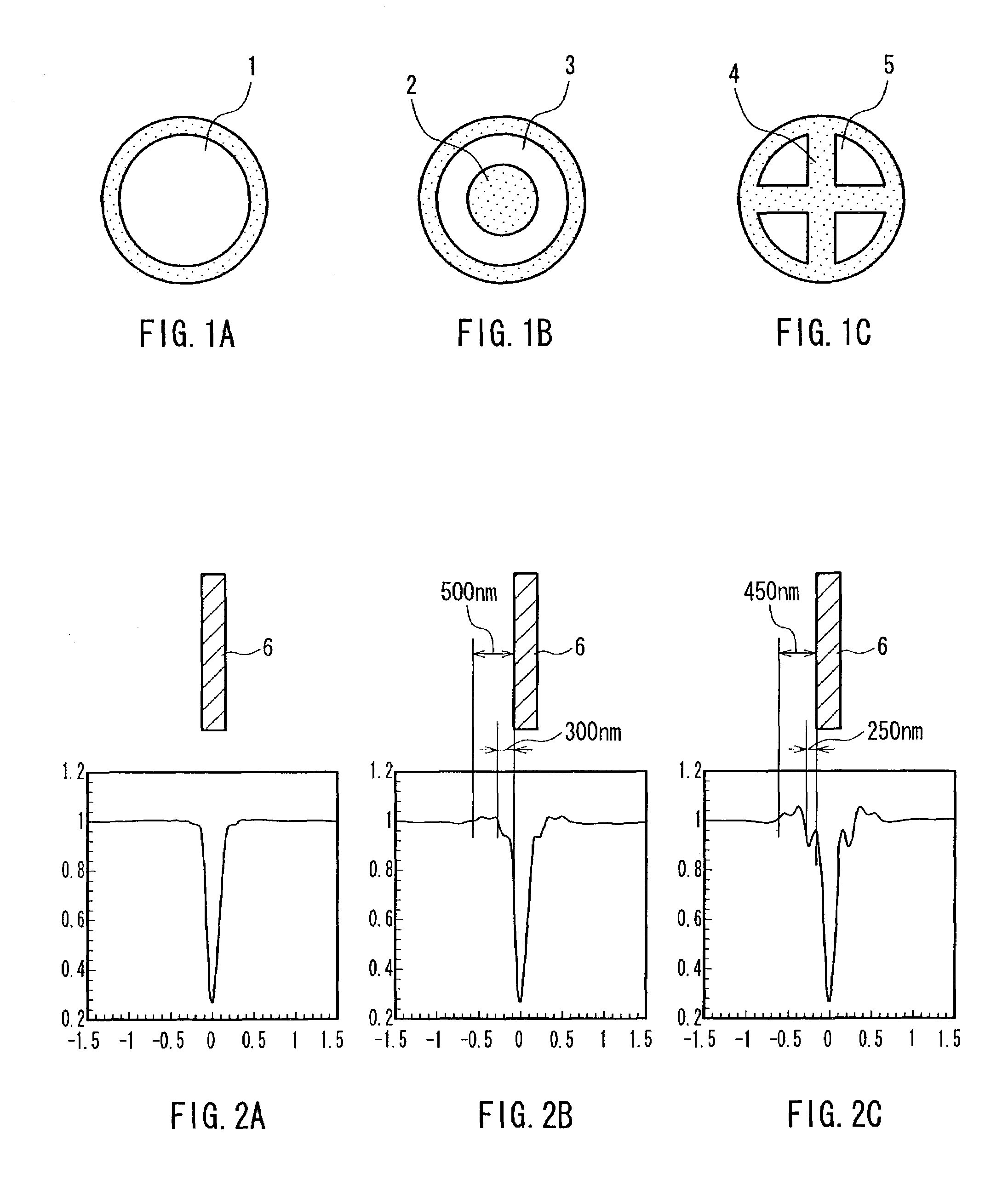
[0035]Embodiment 1 will be described by referring to FIGS. 4A and 4B, FIGS. 5A and 5B, and FIG. 6. FIGS. 4A and 4B are plan views, each showing pattern data used for forming a mask of this embodiment. In the pattern data of FIGS. 4A and 4B, a diagonally shaded region 10 corresponds to a light-shielding portion for shielding off-axis illumination light, and a plain region 11 corresponds to a light-transmitting portion for transmitting the off-axis illumination light. FIGS. 5A and 5B are plan views showing resist patterns formed by the mask based on the pattern data in FIGS. 4A and 4B, respectively. FIG. 6 is a graph showing a portion of the contour of the resist pattern formed by ⅔ annular illumination.

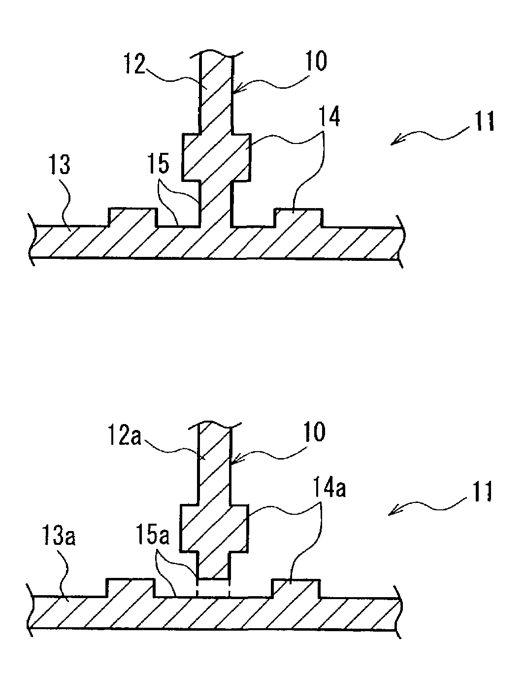
[0036]The pattern data of FIG. 4A includes a junction at which line circuit patterns 12, 13 (line width: about 100 nm) are connected to each other with the circuit pattern 12 being orthogonal to the circuit pattern 13 so as to form a T-shape. A rectangular small pattern 14 having a wid...

embodiment 2

[0046]Embodiment 2 will be described by referring to FIG. 7. FIG. 7 is a graph showing a portion of the contour of a resist pattern formed by quadrupole illumination. In this embodiment, a mask including a 10 nm-wide small pattern was produced, and quadrupole illumination was used for exposure. The pattern etc. of the mask used are the same as those shown in FIGS. 4A, 4B, 5A, and 5B of Embodiment 1.

[0047]FIG. 7 shows the specific shape of a vertical line pattern in the vicinity of the junction of the resist pattern in comparison with conventional examples. The horizontal and vertical axes (nm) of this graph are the same as FIG. 6. A conventional example B1 shows a case using the same mask pattern and transfer conditions as those of this embodiment, except that no small pattern is formed. A conventional example B2 shows a case using a 10 nm-wide small pattern in the same manner as this embodiment, except that the small pattern is formed within the range between 0.4 and 0.75 λ / (NA·K) ...


PUM


Abstract

A photomask is used for transferring a mask pattern onto a semiconductor substrate. The mask pattern includes a junction at which two line patterns are connected to each other with one line pattern being orthogonal to the other line pattern so as to form a T-shape, or a proximity portion at which two line patterns are located close to each other with one line pattern being substantially orthogonal to the other line pattern so as to form a T-shape. A small pattern is formed on a side edge of the line pattern in the vicinity of the junction or the proximity portion so as to form a wide portion of the line pattern. The small pattern is provided within the range between 0.79 and 1.8 λ / (NA·K) of a distance from the neighboring side edge of the other line pattern, where λ is the wavelength of exposure illumination light, NA is the numerical aperture of a lens used, and K is a transfer reduction ratio.

Description

BACKGROUND OF THE INVENTION[0001]1. Field of the Invention[0002]The present invention relates to a photomask and a pattern forming method.[0003]2. Description of the Related Art[0004]With the recent progress in miniaturization of semiconductor devices, the semiconductor devices with 50 to 150 nm design rules have been developed. A photolithography process in the manufacture of a semiconductor device uses light in the near-ultraviolet or ultraviolet region as an exposure light source, e.g., G-rays (wavelength: 436 nm), i-rays (wavelength: 365 nm), a KrF excimer laser (wavelength: 248 nm), an ArF excimer laser (wavelength: 193 nm), or an F2 laser (wavelength: 156 nm). At present, a KrF excimer laser beam or ArF excimer laser beam is used to form a resist pattern having a smaller line width on a semiconductor substrate.[0005]An exposure technique that uses such high-energy light with off-axis illumination, a phase shift mask, etc. is generally known as a super-resolution technique. The...

Claims


Application Information

Patent Timeline
IPC IPC(8): G03F1/00G03F1/36G03F7/20
CPCG03F1/144G03F1/36G03F7/70441
Inventor KOIZUMI, TAICHIMISAKA, AKIO
Owner PANASONIC CORP
Why Eureka
Try Eureka