
Field effect transistor

a field effect transistor and transistor technology, applied in watering devices, separation processes, filtration separation, etc., can solve the problems of linearity degradation of mutual conductance (gm), drain conductance degradation (gd), etc., to achieve satisfactory drain conductance (gd), and suppress degradation of linearity of mutual conductance (gm)

Active Publication Date: 2005-09-20
MITSUBISHI ELECTRIC CORP
View PDF6 Cites 4 Cited by
  • Summary
  • Abstract
  • Description
  • Claims
  • Application Information

AI Technical Summary

Benefits of technology

[0010]The present invention has been made to solve the foregoing problems. A first object of the present invention is to configure a field effect transistor which suppresses degradation of linearity of mutual conductance (gm) and provides satisfactory drain conductance (gd), even when a gate bias that reaches near pinch off is applied.
[0011]According to one aspect of the invention, there is provided a field effect transistor according to the present invention comprising: a semi-insulating semiconductor substrate; a semiconductor layer structure provided on the semiconductor substrate, the semiconductor layer structure including a non-doped first compound semiconductor layer, an n-type second compound semiconductor layer having an impurity doping density ranging from 1×1017 cm−3 to 1×1018 cm−3 and a layer thickness ranging from 1 nm to 10 nm and having an energy level at a lower end of a conduction band thereof, which is less than or equal to an energy level at a lower end of a conduction band of the first compound semiconductor layer, and an n-type third compound semiconductor layer having an energy level at a lower end of a conduction band thereof, which is less than the energy level at the lower end of the conduction band of the second compound semiconductor layer, the non-doped first compound semiconductor layer, the n-type second compound semiconductor layer and the n-type third compound semiconductor layer being sequentially disposed on the semiconductor substrate from the semiconductor substrate side; and a gate electrode disposed on the semiconductor layer structure, and a source electrode and a drain electrode, the source electrode and the drain electrode being opposite to each other with the gate electrode interposed therebetween and being disposed over the semiconductor layer structure. Owing to the configuration referred to above, the second compound semiconductor layer is perfectly depleted. To this end, electrons in the second compound semiconductor layer are diffused into the third compound semiconductor layer side in the neighborhood of an interface between the second compound semiconductor layer and the third compound semiconductor layer. Thus, an electron density distribution at the third compound semiconductor layer in the vicinity of the interface between the second compound semiconductor layer and the third compound semiconductor layer is enhanced.
[0012]Accordingly, the present invention is advantageous in that the degradation in linearity of mutual conductance (gm) is suppressed even in a bias voltage region in which the absolute value of a gate bias corresponding to a negative voltage becomes large and thereby reaches near pinch off, and further in that a satisfactory value of drain conductance (gd) can be obtained.
[0013]By extension, a high output amplifier good in amplifying characteristic and having less distortion can be provided at low cost in the simple configuration that an electron supply layer is interposed between a buffer layer and a channel layer.

Problems solved by technology

However, a problem arises in that when the absolute value of the gate bias corresponding to the negative voltage becomes large and thereby reaches near pinch off, degradation of linearity of mutual conductance (gm) and deterioration of drain conductance (gd) occur.

Method used


Image

  • Field effect transistor
  • Field effect transistor
  • Field effect transistor

Examples


first embodiment

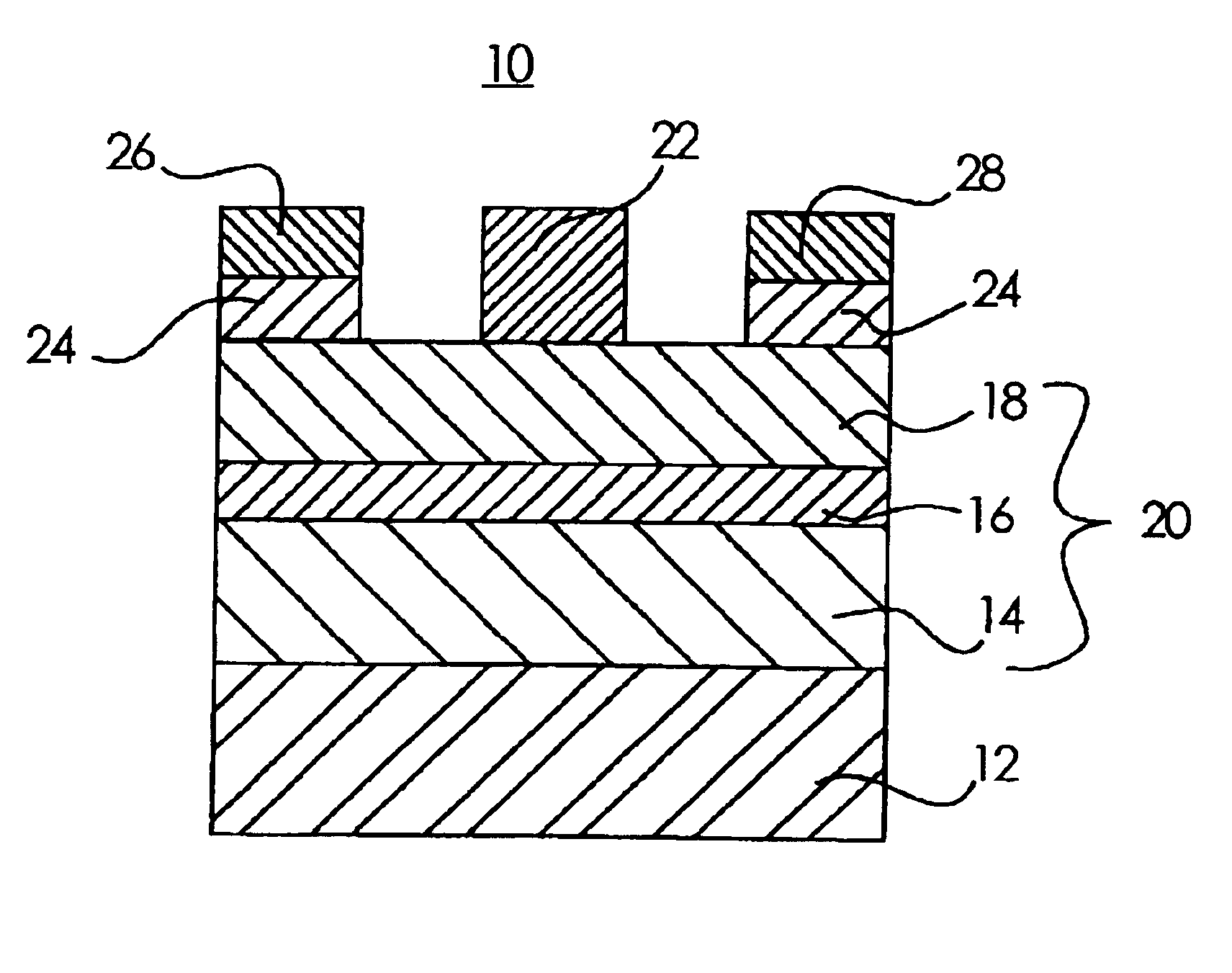
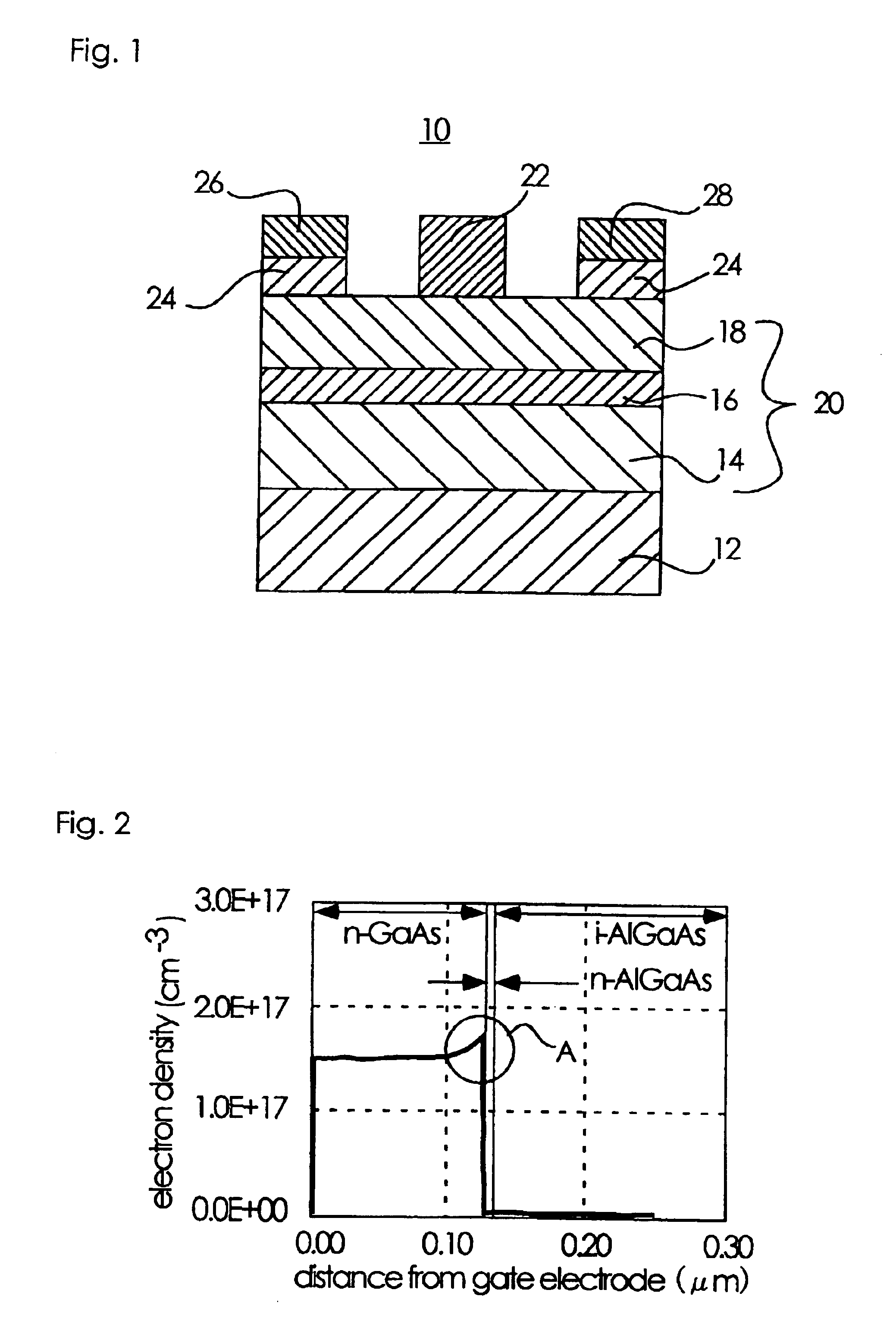
[0025]FIG. 1 is a cross-sectional view of a field effect transistor according to an embodiment of the present invention.

[0026]In FIG. 1, the MESFET 10 makes use of a semi-insulating GaAs substrate 12 used as a semi-insulating semiconductor substrate. In the MESFET 10, a non-doped AlGaAs buffer layer 14 (hereinafter, the term non-doped is expressed in “i-” and the term n conductivity type is expressed in “n-”) used as a non-doped first compound semiconductor layer is disposed on the GaAs substrate 12. The thickness Tb of the buffer layer 14 ranges from about 10 nm to about 500 nm. An electron supply layer 16 made of n-AlGaAs, which is used as a second compound semiconductor layer, is provided on the buffer layer 14.

[0027]The electron supply layer 16 is one formed on condition that a doping impurity is Si, an impurity doping density Nde is set to 1×1017 cm−3 to 1×1018 cm−3 (e.g., 1×10¹⁷ is hereinafter expressed in 1E17), more preferably, 1.5E17 cm−3 to 5E17 cm−3, and the thickness Te ...

modification 1

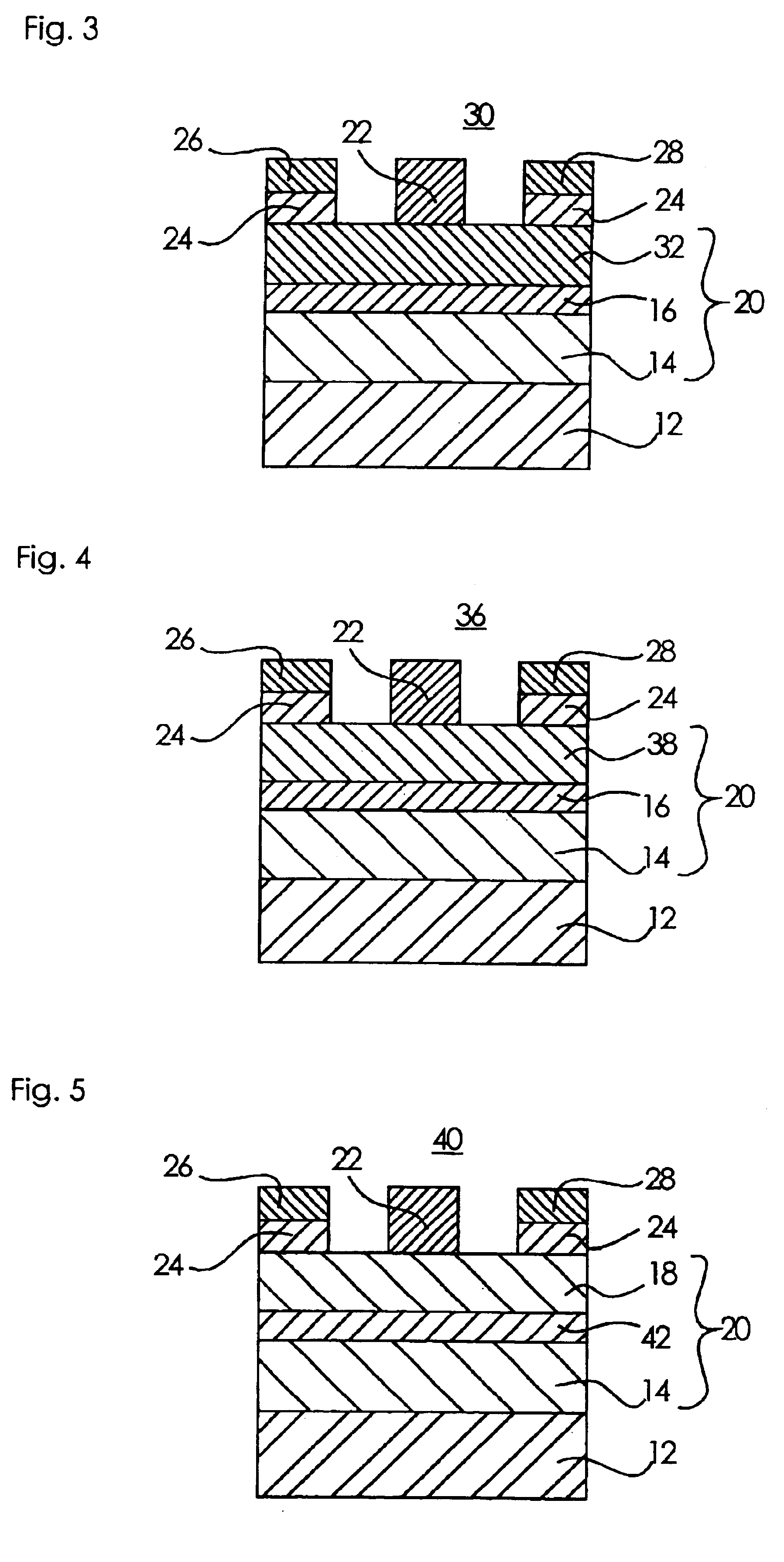
[0048]FIG. 3 is a cross-sectional view of a field effect transistor illustrative of one modification of an embodiment of the present invention. In FIG. 3, the same reference numerals as those shown in FIG. 1 are the same ones or equivalent ones. Further, the following respective drawings are also similar to the above.

[0049]In FIG. 3, the MESFET 30 is different from the MESFET 10 shown in FIG. 1 in that the MESFET 30 makes use of an n-InGaAs channel layer 32 as an alternative to the n-GaAs channel layer 18 of the MESFET 10. The MESFET 30 is identical to the MESFET 10 in other configuration.

[0050]Even in the case where the n-InGaAs channel layer 32 is used, the channel layer 32 is set in such a manner that its layer thickness Tc ranges from 10 nm to 50 nm, a doping impurity is taken as Si, and an impurity doping density thereof ranges from about 5E16 cm−3 to about 1E18 cm−3.

[0051]Therefore, the relations among the expressions (1), (2) and (3) are satisfied.

[0052]In the present MESFET ...

modification 2

[0053]FIG. 4 is a cross-sectional view of a field effect transistor illustrative of one modification of an embodiment of the present invention.

[0054]In FIG. 4, the MESFET 36 is different from the MESFET 10 shown in FIG. 1 in that the MESFET 36 takes an Al composition ratio x of AlGaAs of an electron supply layer 16 as x≧0.27 and makes use of an n-In0.5Ga0.5P channel layer 38 as an alternative to the n-GaAs channel layer 18 of the MESFET 10. The MESFET 36 is identical to the MESFET 10 in other configuration.

[0055]Even when the n-In0.5Ga0.5P channel layer 38 is used, the channel layer 38 is set in such a manner that its layer thickness Tc ranges from 10 nm to 50 nm, a doping impurity is taken as Si, and an impurity doping density thereof ranges from about 5E16 cm−3 to about 1E18 cm−3.

[0056]Also the electron supply layer 16 simply varies slightly in Al composition ratio and is identical to the MESFET 10 in other condition. The Al composition ratio is limited because lattice matching wi...


PUM

PropertyMeasurementUnit
Carrier concentrationaaaaaaaaaa
Energy levelaaaaaaaaaa
Semiconductor propertiesaaaaaaaaaa

Abstract

An MESFET is configured wherein a semiconductor layer structure including an i-AlGaAs buffer layer, an n-AlGaAs electron supply layer having an impurity doping density ranging from 1×1017 cm−3 to 1×1018 cm−3 and a layer thickness ranging from 1 nm to 10 nm, and an n-GaAs channel layer, all of which are sequentially deposited from the semi-insulating GaAs substrate side, is disposed on the semi-insulating GaAs substrate, a gate electrode is provided on the n-GaAs channel layer, and a source electrode and a drain electrode opposite to each other with the gate electrode interposed therebetween are provided.

Description

BACKGROUND OF THE INVENTION[0001]1. Field of the Invention[0002]The present invention relates to a field effect transistor, and particularly to a field effect transistor used in a high output amplifier of a mobile communication base station, an artificial satellite or the like.[0003]2. Description of the Related Art[0004]The quality of transferred sound, and the like, as well as merely, reduction in size and weight, become important point in the development of a recent portable terminal such as a cellular phone. There is a need to transfer a signal with less distortion upon improving sound quality. It is important for a high output power amplifier such as a mobile communication base station to provide a less reduction in distortion at its amplifying characteristic in addition to gain as one important item for achieving the above. Similarly, a satellite's onboard high output amplifier used in satellite communications or the like needs to be simply brought into not only less weight an...

Claims


Application Information

Patent Timeline
IPC IPC(8): H01L29/66H01L29/778H01L21/02H01L21/338H01L31/0264H01L31/0328H01L29/812H01L31/0304H01L21/335
CPCH01L29/7781H01L29/812B01D29/085B01D35/02A01G25/00B01D2201/347
Inventor NAKAMOTO, TAKAHIRO
Owner MITSUBISHI ELECTRIC CORP
Learn More